Profile confinement to improve transistor performance

a profile confinement and transistor technology, applied in the direction of transistors, semiconductor devices, electrical apparatus, etc., can solve the problems of reducing the vertical junction depth and suppressing the lateral diffusion of dopant in order to control short-channel characteristics, degrading the drive current, and difficult to confine boron/bfsub>2 /sub, so as to improve the neutralization ability, improve the profile of source/drain regions, and reduce the diffusion of p-type impur

Active Publication Date: 2006-11-02
TRENCHANT BLADE TECH LLC
View PDF23 Cites 34 Cited by
  • Summary
  • Abstract
  • Description
  • Claims
  • Application Information

AI Technical Summary

Benefits of technology

[0008] In accordance with one aspect of the present invention, a method of forming a semiconductor device (transistor) having a well-confined profile is provided. The method includes forming a lightly diffused source / drain (LDD) region and a heavily doped source / drain (N+ S / D) region. A p-type pocket / halo region is formed preferably along a channel-side border of the N+ S / D region, to neutralize diffused n-type elements from the N+ S / D region. A diffusion-retarding region is formed to retard diffusion of both p-type and n-type impurities. The diffusion-retarding region is preferably tilt implanted to extend under the gate electrode. More than one pocket / halo region can be formed through multiple implants so that a customized contour of p-type impurities can be formed. This in turn improves the profile of the N+ S / D region. The diffusion-retarding region is also preferably formed in the gate electrode. This reduces the diffusion of n-type impurities into the gate dielectric, and thus preserves gate oxide integrity.
[0010] The diffusion-retarding region retards the diffusion of the n-type impurities of the source / drain regions, enabling high concentrations in the LDD and N+ S / D regions. The p-type impurity diffusion is also reduced, forming regions with higher concentration of p-type impurities. Higher concentration of p-type impurities in turn improves the neutralization ability, and thus further improves the profile of source / drain regions. Therefore, the gate oxide integrity, threshold voltage-control and drain saturation current of the resulting semiconductor devices are improved.

Problems solved by technology

As the dimensions of transistors are scaled down, the reduction of vertical junction depth and suppression of dopant lateral diffusion in order to control short-channel characteristics become greater challenges.
However, it is difficult to confine the boron / BF2 within desired locations to effectively neutralize the lateral diffusion of the n-type dopants.
The activation of the source / drain impurities, however, is affected, resulting in degraded drive current.
However, these approaches are effective only in suppressing vertical diffusion.
The same approaches are less effective in suppressing lateral diffusion of the dopants into the channel region.

Method used


Image

  • Profile confinement to improve transistor performance
  • Profile confinement to improve transistor performance
  • Profile confinement to improve transistor performance

Examples


Embodiment Construction

[0017] The making and using of the presently preferred embodiments are discussed in detail below. It should be appreciated, however, that the present invention provides many applicable inventive concepts that can be embodied in a wide variety of specific contexts. The specific embodiments discussed are merely illustrative of specific ways to make and use the invention, and do not limit the scope of the invention.

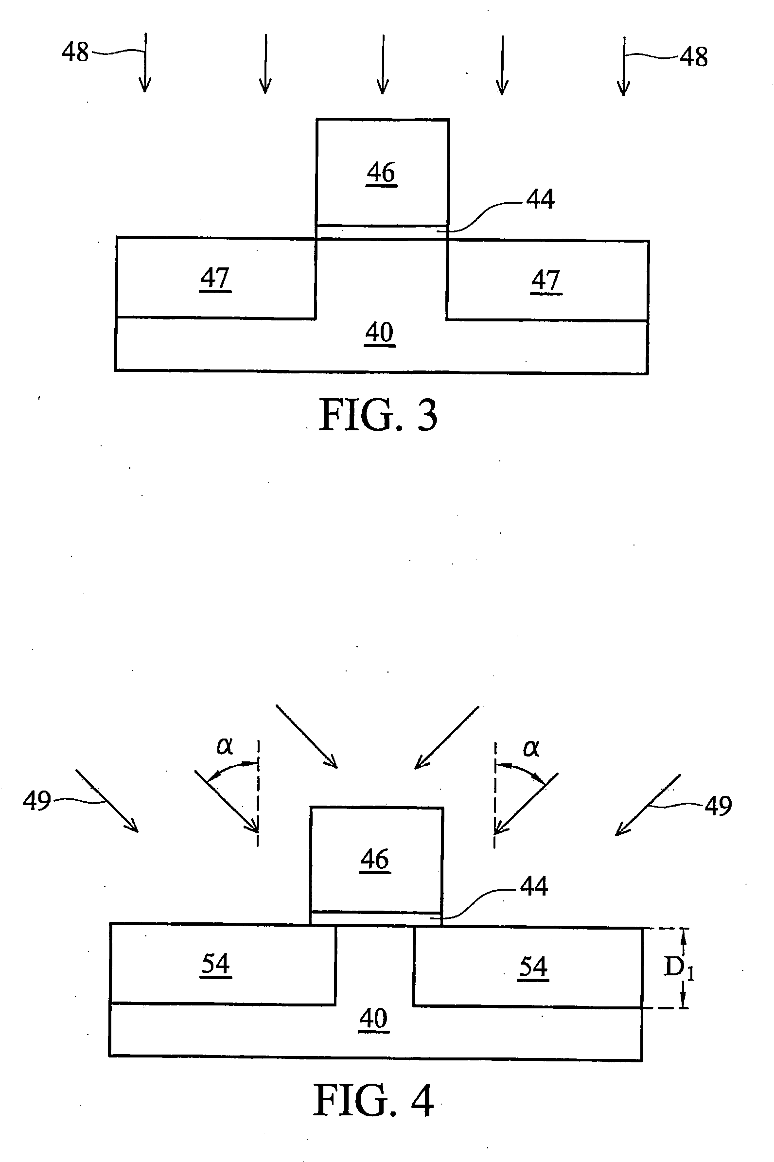
[0018] In order to manufacture an nMOS device with a well-confined profile, greater abruptness of n-type impurities, which means that the impurity regions have well-defined borders, in respective source / drain regions are preferred. The preferred embodiments of the present invention use p-type impurities to neutralize the n-type diffusion. Since p-type impurities also out-diffuse, the effectiveness of the neutralization is reduced. This problem is also addressed by the preferred embodiments of the present invention.

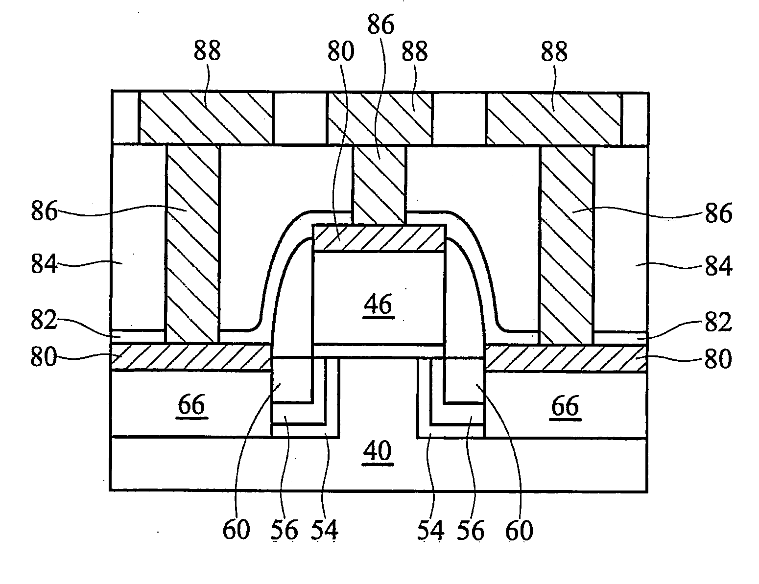
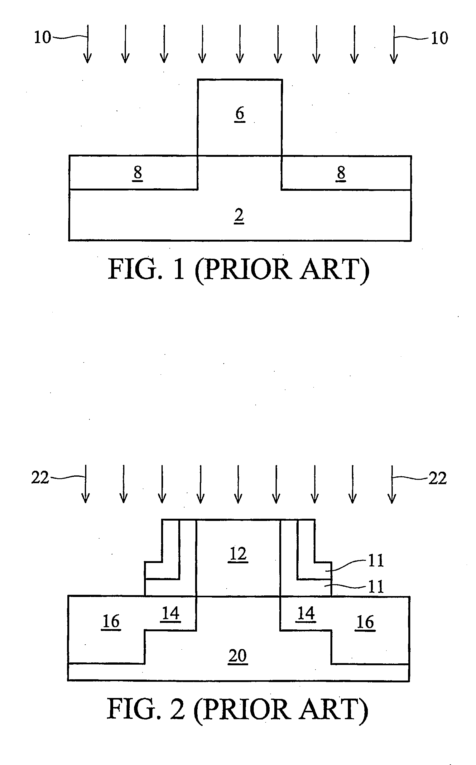
[0019] The cross sectional views of the intermediate stages...


PUM


Abstract

A semiconductor device having well-defined profiles is disclosed. A p-type pocket / halo region is preferably formed along a channel-side border of the heavily doped source / drain region to neutralize diffused n-type elements. A diffusion-retarding region is formed to retard diffusion for both p-type and n-type impurities by substantially overlapping or extending beyond the p-type pocket / halo region and the N+ S / D region at least on the channel side.

Description

TECHNICAL FIELD [0001] This invention relates generally to transistor manufacturing processes, and more specifically to profile confinement of source / drain regions and gates. BACKGROUND [0002] As the dimensions of transistors are scaled down, the reduction of vertical junction depth and suppression of dopant lateral diffusion in order to control short-channel characteristics become greater challenges. The implant of p-type dopants (impurities), such as boron, BF2, and indium is typically needed to neutralize lateral diffusion of n-type impurities (arsenic, phosphorus, etc.) from source / drain regions, and to keep the short channel effect under control. [0003] However, it is difficult to confine the boron / BF2 within desired locations to effectively neutralize the lateral diffusion of the n-type dopants. Having high diffusibility, boron and BF2 dopants diffuse away easily from original implanted regions during subsequent processes that require elevated temperatures, such as rapid therm...

Claims


Application Information

Patent Timeline
Patent Type & Authority Applications(United States)
IPC IPC(8): H01L29/76
CPCH01L21/26506H01L21/26586H01L29/1045H01L29/7843H01L29/665H01L29/6659H01L29/1083H01L21/2658
Inventor CHEN, CHIEN-HAONIEH, CHUN-FENGMAI, KARENLEE, TZE-LIANG
Owner TRENCHANT BLADE TECH LLC
Why Eureka
Try Eureka