Apparatus and methods for scatterometry of optical devices

a technology of optical devices and apparatus, applied in the direction of measurement devices, semiconductor devices, instruments, etc., can solve the problems of insufficient pc structure measurement, complex return radiation pattern, and less than optimal led performan

Inactive Publication Date: 2006-11-02
NANOMETRICS
View PDF5 Cites 40 Cited by
  • Summary
  • Abstract
  • Description
  • Claims
  • Application Information

AI Technical Summary

Problems solved by technology

One challenge in manufacturing photonic crystals for use with LEDs is that the structure of the photonic crystal scattering features has a strong influence on the performance of the crystal itself.
Furthermore, if the shape or position of the scattering features is not optimal, the performance of the LED will also be less than optimal.
Another challenge in the manufacture of photonic crystal for use with LEDs is alignment of the photonic crystal with the LED emission region.
One challenge of scatterometry for the measurement of photonic crystal structures is properly locating the small scattering structures on the workpiece.
Another challenge of using scatterometry to evaluate PC structures is obtaining a useful representation of the radiation returning from such microstructures.
Because the PC structures are typically more complicated than semiconductor structures, the returning radiation pattern may be complex.
Hence, a scatterometer that measures returning radiation in one plane only is sufficient for semiconductor applications, but may be inadequate for the measurement of PC structures.
Another challenge of assessing PC structures using scatterometry relates to the optical properties of the materials that are used to manufacture such structures.
The fact that a PC-LED substrate is non-absorbing creates difficulties in managing back-reflections from the back-side of the substrate and other layers.
In contrast to semiconductor applications, where there is no back-side reflection because all the radiation is absorbed, back-reflections for PC-LED applications can interfere with the incident illumination and therefore alter the returning or scattered radiation.

Method used


Image

  • Apparatus and methods for scatterometry of optical devices
  • Apparatus and methods for scatterometry of optical devices
  • Apparatus and methods for scatterometry of optical devices

Examples


Embodiment Construction

A. Overview

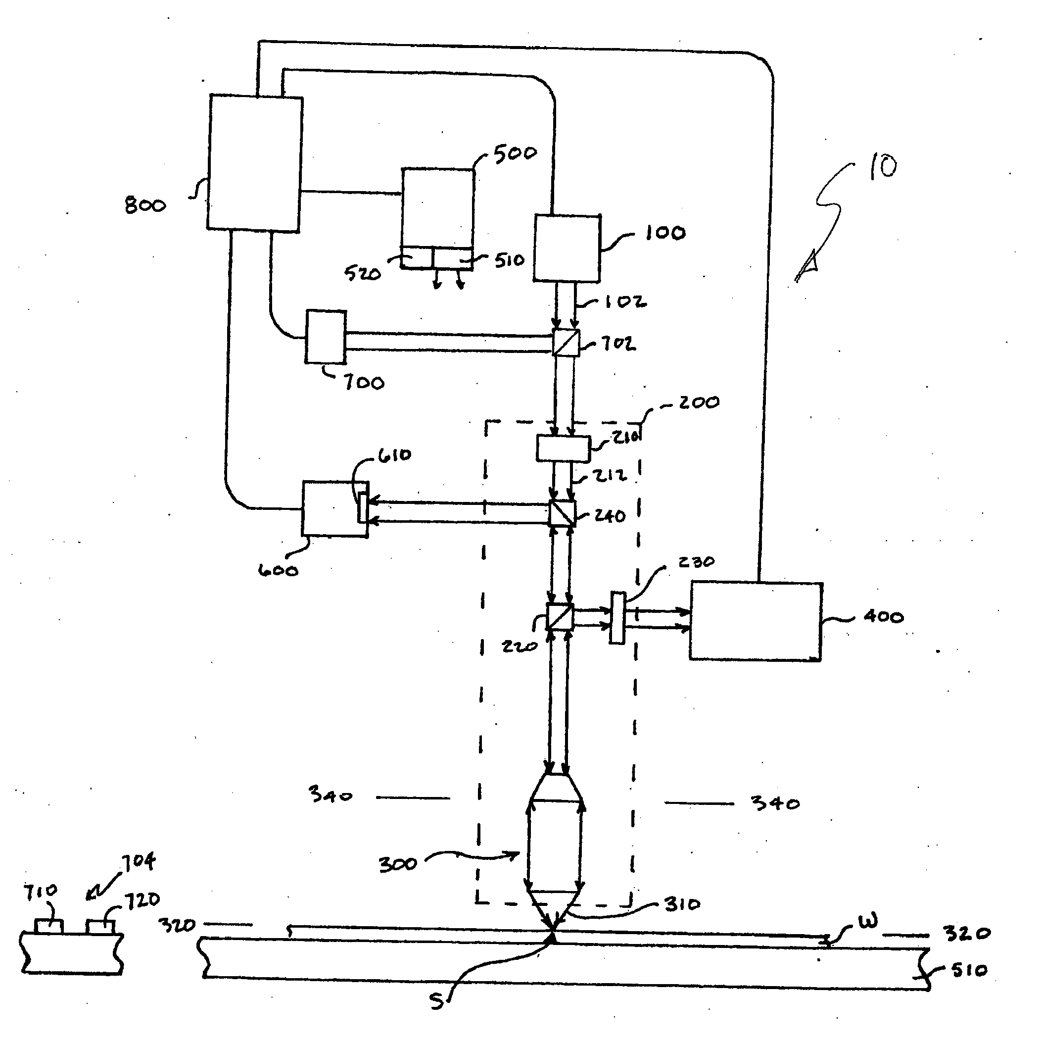
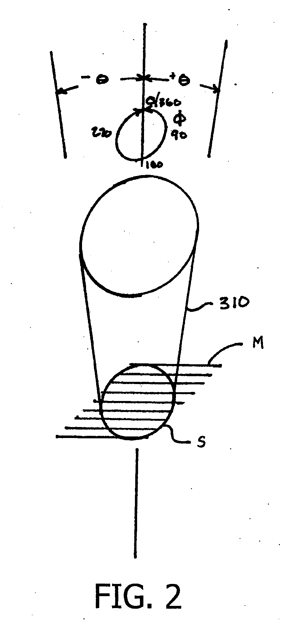
[0034] The present invention is directed toward evaluating photonic crystal (PC) microstructures on optical workpieces and other types of substrates. Many applications of the present invention are directed toward scatterometers and methods of using scatterometry to determine several parameters of periodic microstructures, pseudo-periodic structures, and other very small structures having features sizes as small as 100 nm or less. Several specific embodiments of the present invention are particularly useful in the semiconductor industry to determine the width, depth, line edge roughness, wall angle, film thickness, and many other parameters of the features formed in microprocessors, memory devices, and other semiconductor devices. The scatterometers and methods of the invention, however, are not limited to semiconductor applications and can be applied equally well in other applications.

[0035] One embodiment of the invention is directed toward a scatterometer for evaluatin...


PUM

PropertyMeasurementUnit
widthaaaaaaaaaa
sizesaaaaaaaaaa
azimuth anglesaaaaaaaaaa

Abstract

In a method for measuring a dimension or angle of a scattering feature of an optical device, such as a photonic crystal, at least part of the array is irradiated with light. A characteristic of light scattered from the array is detected. A comparison algorithm is run on the detected characteristic of the scattered light. The comparison algorithm provides one or more numerical values indicative of the measured dimension or angle. A system for measuring a dimension or angle of a feature of an optical device includes a light source and optics for focusing light from the light source onto a target area of the optical device. A light detector is positioned to detect scattered light from the target area, with the detected light used to create a measured light characteristic. A computer linked to the light detector performs a comparison algorithm on the measured light characteristic and outputs a numerical value of the dimension or angle measured. In method for designing an optical device, such as a photonic crystal for use on an LED, an intended scattered response based on light emission characteristics desired from the optical device is simulated. One or more design parameters of the optical device are varied. An interim reflectance response of the optical device with variation of the parameters is determined. Interim scattered responses are compared to the intended scattered response. One or more scattered responses which match the intended scattered response are selected. An optical device is designed using one or more of the design parameters associated with the selected interim scattered response.

Description

[0001] This Application claims priority to U.S. Provisional Patent Application No. 60 / 669,787 filed Apr. 7, 2005. The field of the invention is optical devices and measuring features of optical devices, such as photonic crystals and LEDs.TECHNICAL FIELD Background [0002] Semiconductor devices, light emitting diodes (LEDs) and other optical or microelectronic devices are typically manufactured on a workpiece having a large number of individual dies (e.g., chips or devices). Each wafer undergoes several different procedures to construct the switches, capacitors, conductive interconnects, filters and other components of the device. For example, a workpiece can be processed using lithography, implanting, etching, deposition, planarization, annealing, and other procedures that are repeated to construct a high density of features. One aspect of manufacturing these devices is evaluating the workpieces to ensure that the microstructures are within the desired specifications. [0003] Photonic...

Claims


Application Information

Patent Timeline
Patent Type & Authority Applications(United States)
IPC IPC(8): G01N21/47
CPCG01N21/47G01N21/4738G01N21/4785H01L2933/0083H01L33/20H01L33/22G01N2021/4735G01N21/95692
Inventor RYAN, TOM W.RAYMOND, CHRISHUMMEL, STEVEN G.
Owner NANOMETRICS
Why Eureka
Try Eureka