Method for fabricating a dual damascene and polymer removal

a dual-damascene and polymer technology, applied in semiconductor/solid-state device manufacturing, basic electric elements, electric apparatus, etc., can solve the problems of increased resistance and rc delays, device defects, and previous cleaning processes that are ineffective in removing polymers from osg and other low-k dielectric sidewalls, etc., to achieve easy removal and low cost

Inactive Publication Date: 2006-11-02
UNITED MICROELECTRONICS CORP
View PDF20 Cites 56 Cited by
  • Summary
  • Abstract
  • Description
  • Claims
  • Application Information

AI Technical Summary

Benefits of technology

[0014] It is an advantage of the claimed invention that the second etching process, the stripping process of the second photoresist layer, the third etching process, and the in-situ dry cleaning process are performed in a same reaction chamber so that the residual polymers formed from the several etching processes can be effectively removed through a simple process and with low cost. The in-situ dry cleaning process includes introducing a cleaning gas, preferably a cleaning gas containing hydrogen (H2), to the reaction chamber where the etching processes are performed to change the composition of the residual polymers so that the polymers with changed composition can be easily removed.

Problems solved by technology

However, there is a serious problem that undesired polymers 40 forming on the surface of the sidewall and bottom of the dual damascene 38 are produced during the above-described etching processes.
However, the recent introduction of low-k materials, such as OSG, in combination with silicon carbide (SiC) etch-stop materials and copper fill materials has rendered previous cleaning processes ineffective in removing polymers from OSG and other low-k dielectric sidewalls.
During the via-first dual damascene process, polymers are also formed on the sidewall and bottom of the dual damascene, which result in device defects such as increased resistance and RC delays.
Similarly, a conventional wet cleaning process has trouble to effectively removing the residual polymers caused by etching the dielectric layers formed with low-k materials and SiC etch-stop layer.
However, how to remove the residual polymers produced by etching the low-k dielectric layer with a more effective and simpler process without destroying the dual damascene is still an important issue that needs to be considered.

Method used


Image

  • Method for fabricating a dual damascene and polymer removal
  • Method for fabricating a dual damascene and polymer removal
  • Method for fabricating a dual damascene and polymer removal

Examples


Embodiment Construction

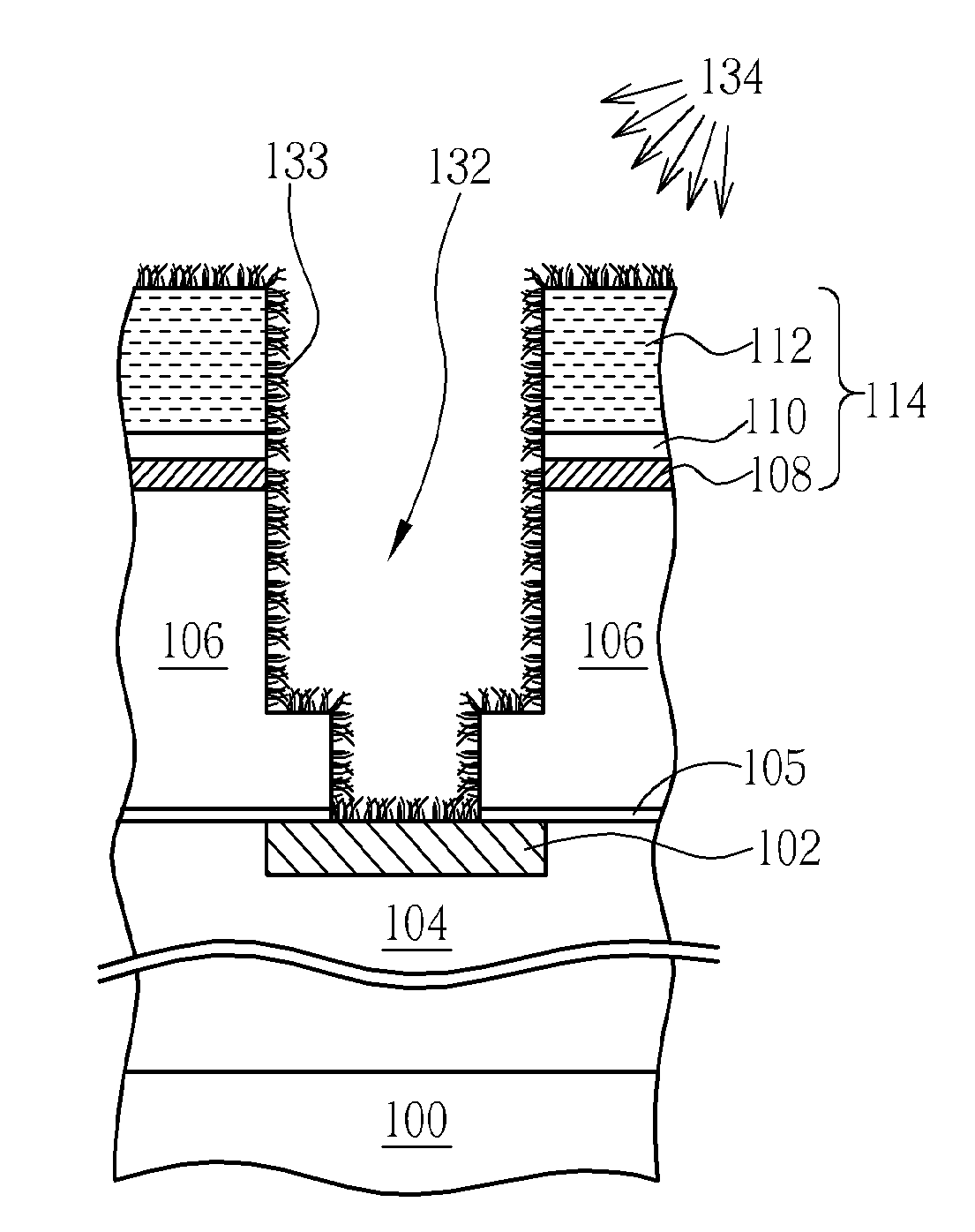
[0018] Please refer to FIGS. 6-11. FIGS. 6-11 are schematic diagrams of a trench-first dual damascene process according to the present invention. As shown in FIG. 6, a semiconductor substrate 100 is provided, wherein the semiconductor substrate 100 has a conductive layer 102 thereon and is positioned in a first dielectric layer 104. Then, a bottom layer 105, a second dielectric layer 106, an etch-stop layer 108, a metal layer 110, a mask layer 112, and a first BARC layer 116 are formed over the first dielectric layer 104 and the conductive layer 102. The etch-stop layer 108, metal layer 110, and the mask layer 112 form a composite layer serving as a hard mask 114 during the follow-up etching processes. The etch-stop layer 108 is a SiC layer. The metal layer 110 is preferably a titanium nitride (TiN) layer or a tantalum nitride (TaN) layer. The mask layer 112 is selectively formed with a plasma enhanced oxide (PEOX) layer. In addition, the bottom layer 105 is a SiN layer, and the sec...


PUM


Abstract

A method for fabricating a dual damascene includes a partial etching process, a photoresist layer stripping process, and a blanket etching process. After the blanket etching process, an in-situ dry cleaning process is performed to remove residual polymers resulting from the etching processes.

Description

CROSS REFERENCE TO RELATED APPLICATIONS [0001] This application is a divisional of application Ser. No. 10 / 905,359 filed Dec. 30, 2004.BACKGROUND OF THE INVENTION [0002] 1. Field of the Invention [0003] The invention relates to a method for fabricating a dual damascene, and more particularly, to a method for fabricating a dual damascene that can effectively remove residual polymers resulting from etching processes. [0004] 2. Description of the Prior Art [0005] To meet the needs of high integration and high processing speed in 0.13 micron generation integrated circuits (ICs), a copper (Cu) interconnect technology has now become an effective solution. Cu is approximately 30% lower in resistivity than Al and has fewer reliability concerns such as electromigration. Cu interconnect technology, by and large, has been implemented employing damascene techniques, wherein an ILD, such as a silicon oxide layer, e.g., derived from tetraethyl orthosilicate (TEOS) or silane, or a low-k material, ...

Claims


Application Information

Patent Timeline
Patent Type & Authority Applications(United States)
IPC IPC(8): H01L21/465
CPCH01L21/02063H01L21/31144H01L21/76814H01L21/76813H01L21/76811
Inventor WANG, JENG-HO
Owner UNITED MICROELECTRONICS CORP
Why Eureka
Try Eureka