Removal of charged defects from metal oxide-gate stacks

Inactive Publication Date: 2006-11-02
IBM CORP
View PDF12 Cites 76 Cited by
  • Summary
  • Abstract
  • Description
  • Claims
  • Application Information

AI Technical Summary

Benefits of technology

[0009] The present invention provides a method for removing charged defects from a material stack, which is useful in forming a pFET device, including at least a high k gate dielectric and a metal contact such that the resultant metal-containing gate stack including said high k gate dielectric has a threshold voltage substantially within the silicon band gap and good carrier mobility. Specifically, the present invention provides a re-oxidation procedure that will restor

Problems solved by technology

The use of noble metals such as Pt are, however, problematic since they suffer from adhesion problem

Method used


Image

  • Removal of charged defects from metal oxide-gate stacks
  • Removal of charged defects from metal oxide-gate stacks
  • Removal of charged defects from metal oxide-gate stacks

Examples


Example

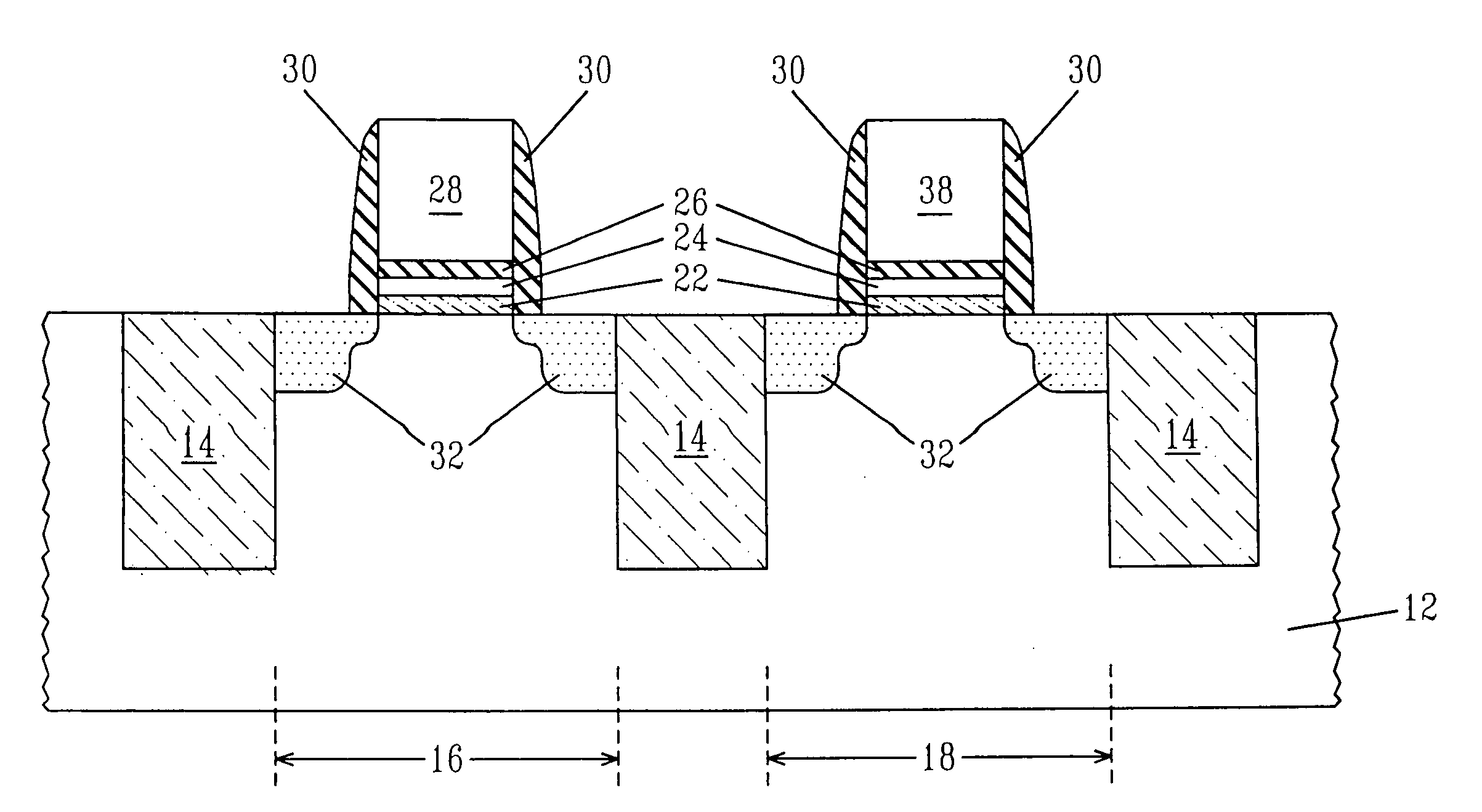
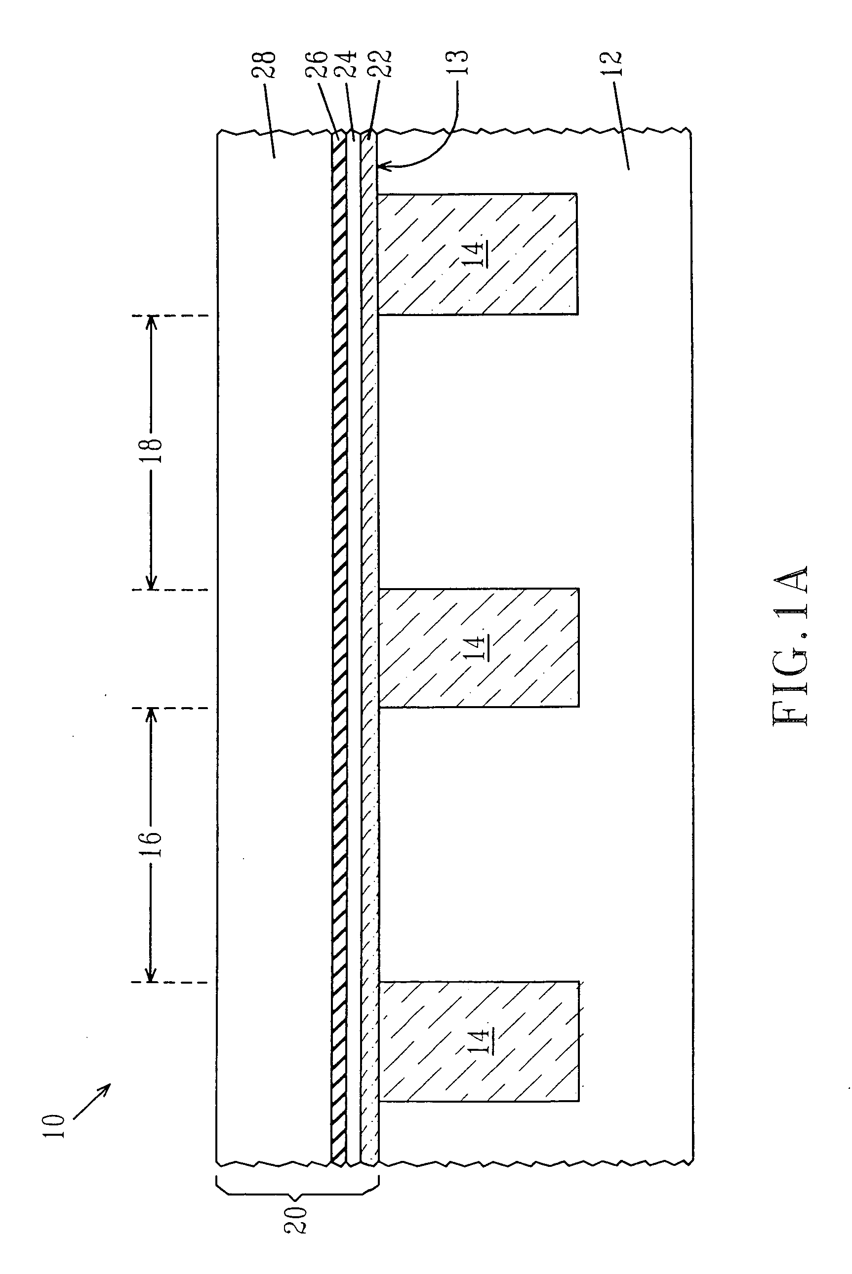
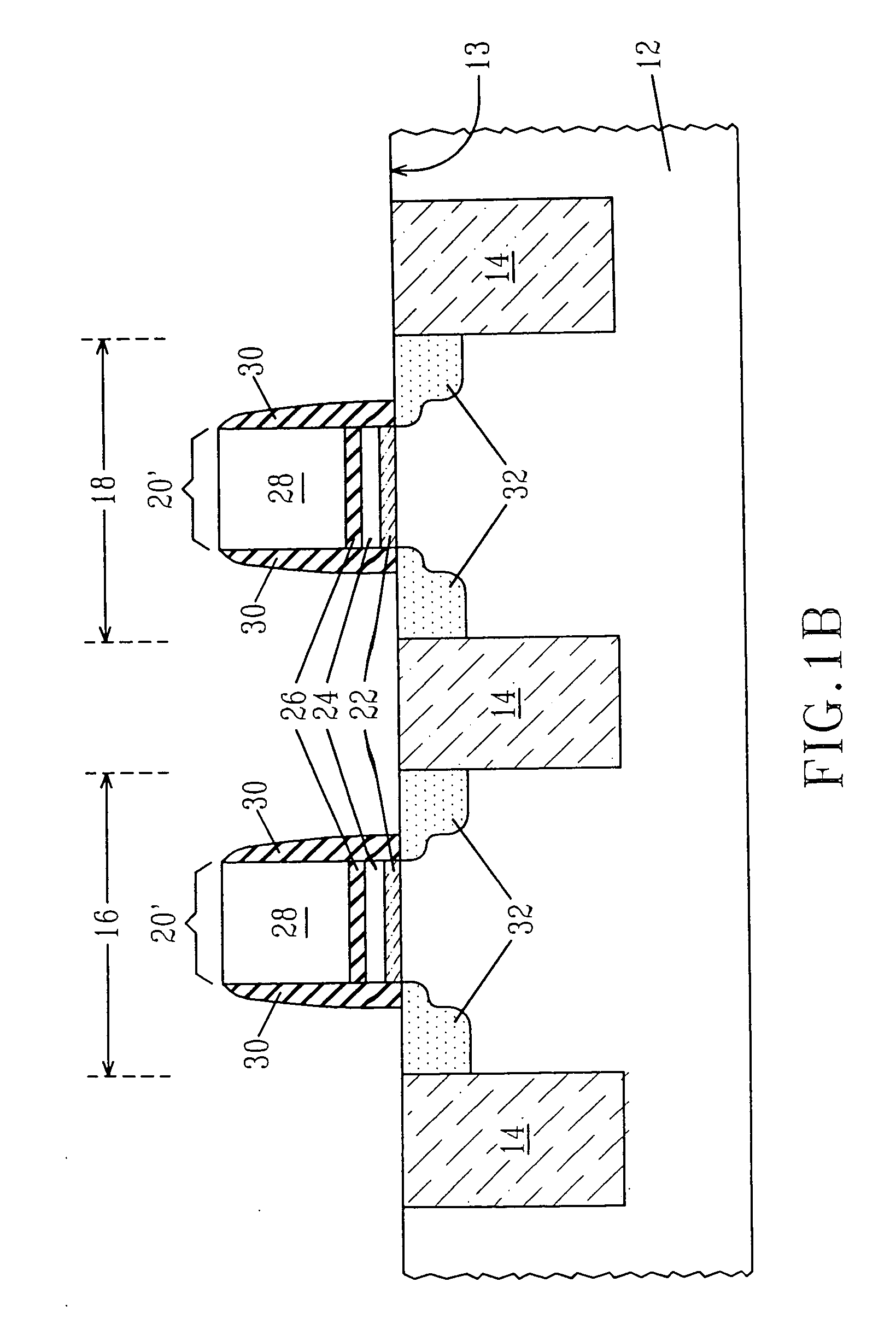
[0025] The present invention, which provides a method of substantially removing charged defects from a material stack including a high k gate dielectric and a metal contact, will now be described in greater detail by referring to the drawings that accompany the present application. It is noted that the drawings of the present application are provided for illustrative purposes and thus they are not drawn to scale.

[0026] Reference is first made to FIGS. 1A-1G which illustrate one of the embodiments of the present invention. It is emphasized that in the drawings of the present application, the semiconductor structure includes both an NFET and a pFET. Although such a structure is shown and described herein below, the present invention also contemplates semiconductor structures that include a pFET, a plurality of pFETs or a combination of a plurality of at least one pFET and at least one NFET. The re-oxidation process described above alters the effective workfunction of the metal contac...


PUM


Abstract

The present invention provides a method for removing charged defects from a material stack including a high k gate dielectric and a metal contact such that the final gate stack, which is useful in forming a pFET device, has a threshold voltage substantially within the silicon band gap and good carrier mobility. Specifically, the present invention provides a re-oxidation procedure that will restore the high k dielectric of a pFET device to its initial, low-defect state. It was unexpectedly determined that by exposing a material stack including a high k gate dielectric and a metal to dilute oxygen at low temperatures will substantially eliminate oxygen vacancies, resorting the device threshold to its proper value. Furthermore, it was determined that if dilute oxygen is used, it is possible to avoid undue oxidation of the underlying semiconductor substrate which would have a deleterious effect on the capacitance of the final metal-containing gate stack. The present invention also provides a semiconductor structure that includes at least one gate stack that has a threshold voltage within a control range and has good carrier mobility.

Description

FIELD OF THE INVENTION [0001] The present invention relates to semiconductor device manufacturing, and more particularly to a method of fabricating a complementary metal oxide semiconductor (CMOS) structure in which the charged defects are substantially removed from a metal oxide gate stack. The present invention also relates to a semiconductor structure that includes at least one gate stack that has a threshold voltage within a control range and has good carrier mobility. BACKGROUND OF THE INVENTION [0002] As is known to those skilled in the semiconductor art, transistors are the main building blocks of integrated circuits (ICs). Modem ICs interconnect millions of densely configured transistors that perform a wide variety of functions. To achieve this densely packed configuration, the physical dimensions of the transistors are typically scaled down to the sub-micron regime. Generally, the transistors used in the sub-micron regime typically include a polysilicon gate. However, polys...

Claims


Application Information

Patent Timeline
IPC IPC(8): H01L21/31
CPCH01L21/28079H01L21/28088H01L21/28176H01L21/28194H01L21/31691H01L21/823462H01L29/7833H01L21/823857H01L29/4958H01L29/513H01L29/517H01L29/66545H01L29/6659H01L21/823842H01L21/02323H01L21/02337
Inventor CARTIER, EDUARD A.COPEL, MATTHEW W.GUHA, SUPRATIKHAIGHT, RICHARD A.MCFEELY, FENTON R.NARAYANAN, VIJAY
Owner IBM CORP
Why Eureka
Try Eureka