Data rewriting method for flash memory using partial erases

a data rewriting and flash memory technology, applied in the direction of memory adressing/allocation/relocation, instruments, digital storage, etc., can solve the problems of wasting a lot of time, so as to achieve the effect of less tim

Inactive Publication Date: 2006-11-02
LAPIS SEMICON CO LTD
View PDF6 Cites 21 Cited by
  • Summary
  • Abstract
  • Description
  • Claims
  • Application Information

AI Technical Summary

Benefits of technology

[0008] An object of the present invention is accordingly to rewrite data in a flash memory in less time than is possible by conventional methods.

Problems solved by technology

Whereas writing takes only a few tens of microseconds, erasing by the conventional method takes a much longer time, typically several tens of milliseconds.
This erasing time is too long for a device such as a contactless smart card, which may need to rewrite data in a time frame shorter than ten milliseconds.

Method used


Image

  • Data rewriting method for flash memory using partial erases
  • Data rewriting method for flash memory using partial erases
  • Data rewriting method for flash memory using partial erases

Examples


first embodiment

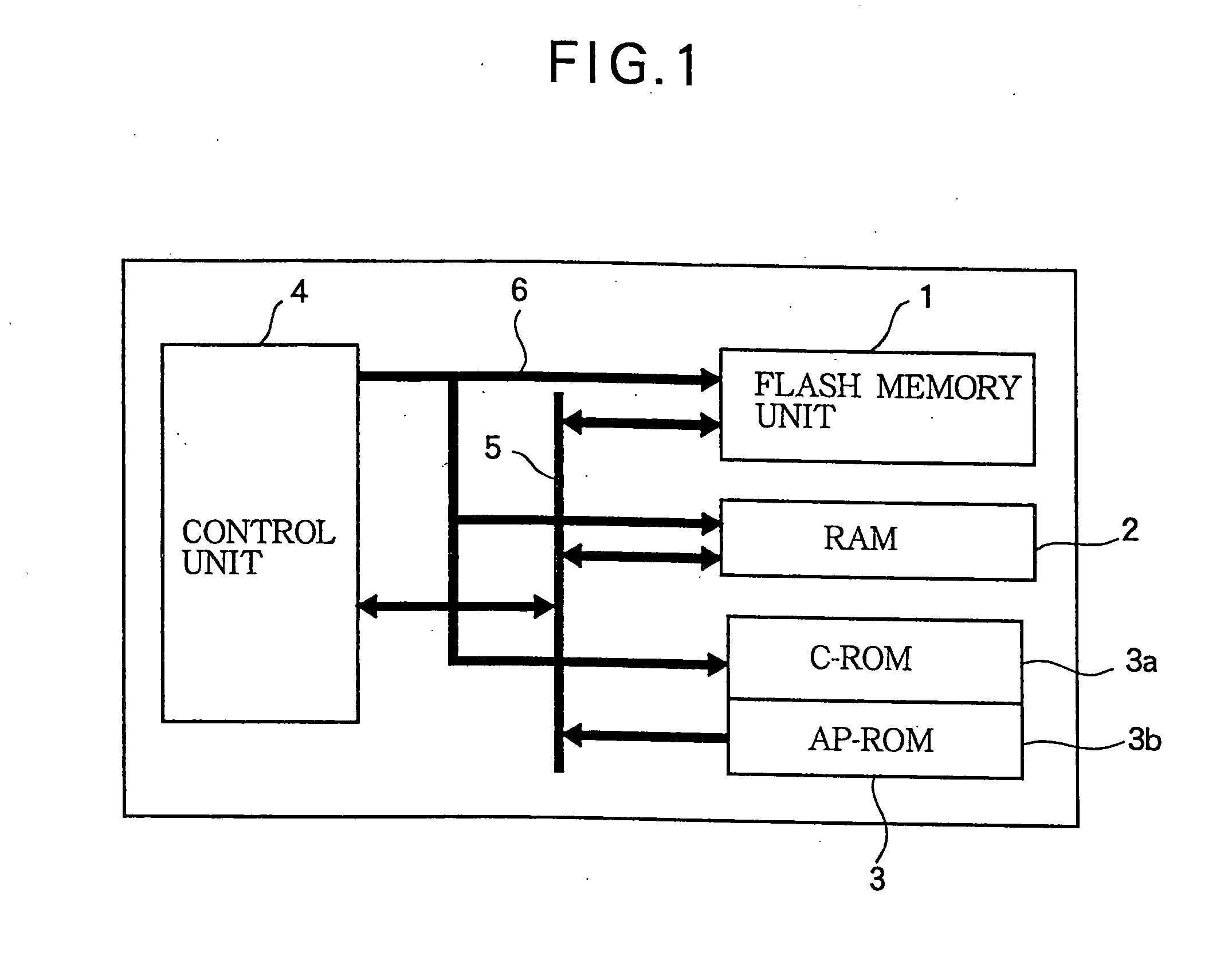
[0028]FIG. 1 is a functional block diagram of a microcomputer illustrating a first embodiment of the invention, comprising a flash memory unit 1, a random-access memory (RAM) 2, a read-only memory (ROM) 3, a control unit 4, a sixteen-bit data bus 5, and a thirteen-bit address bus 6. The ROM 3 includes a control ROM (C-ROM) 3a and an application ROM (AP-ROM) 3b. One function of these component elements is to rewrite data in the flash memory unit 1. The flash memory unit 1 may be embedded in a smart card of the contact type or the contactless type. The flash memory unit 1 and the other component elements may be integrated on a single semiconductor chip, or the flash memory unit 1 may be on a separate chip.

[0029] The flash memory unit 1 stores user data and other data semipermanently. The RAM 2 temporarily stores variables and other work data, such as data awaiting storage in the flash memory unit 1. The ROM 3 stores programs and data that control the operation of the microcomputer: t...

second embodiment

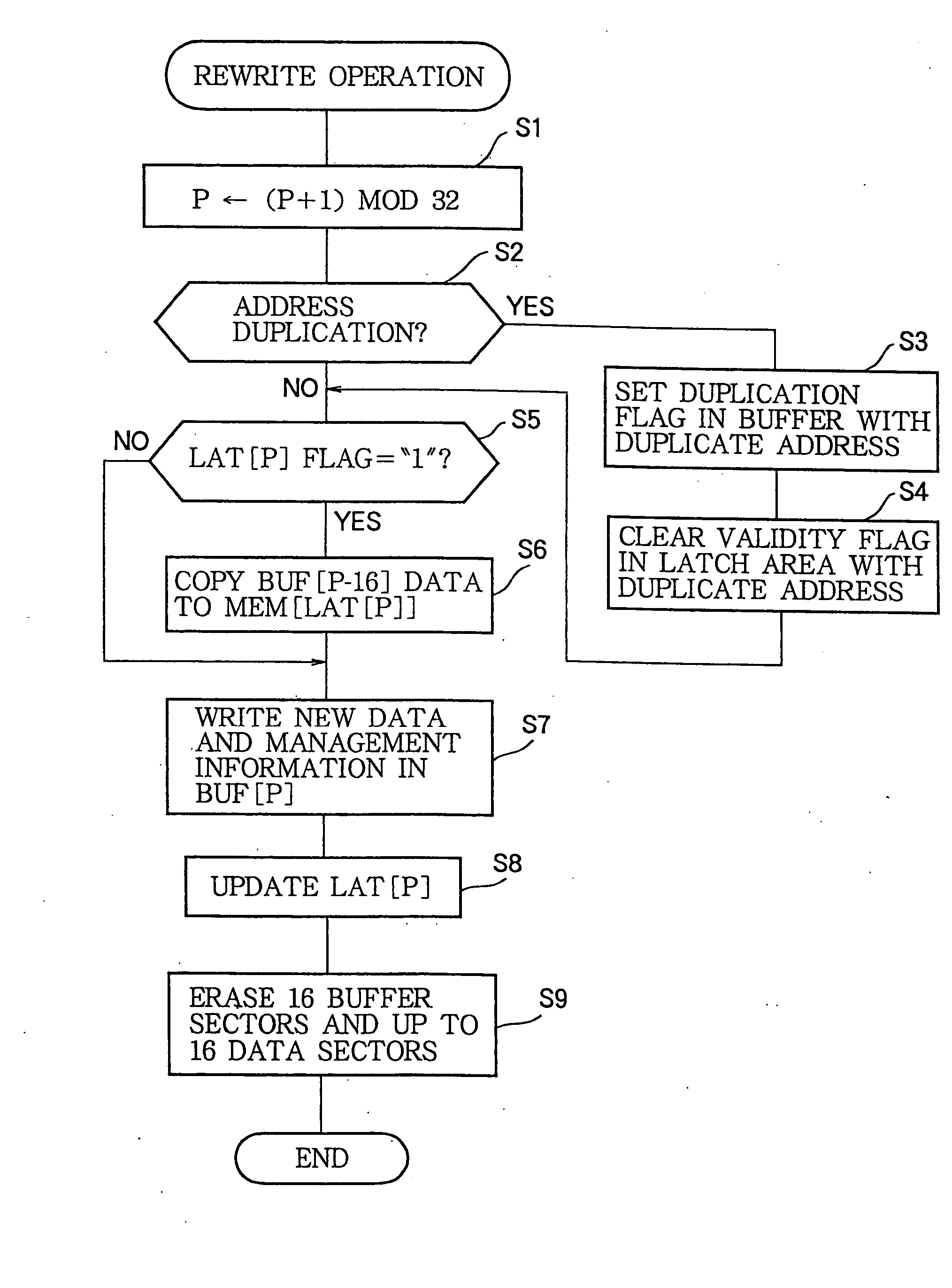
[0115] The rewriting operation in the second embodiment is a variation of the rewriting operation in the first embodiment.

[0116] In the rewriting operation in the first embodiment, if a duplicate address is detected (step S2 in FIG. 10), the duplication flag in the management area 12a of the buffer sector having the duplicate address is set to “1” (step S3), flagging the rewrite address and the old data in that buffer sector as invalid, before the new data and rewrite address have been written in the current buffer sector. If power fails or is shut down during steps S4 to S7, it may therefore become impossible to recover either the new data or the old data. In the rewriting operation of the second embodiment, the duplication flag is not set to “1” until after the new data have been written in the current buffer sector, so that at all times, either the old data or the new data are flagged as valid in the flash buffer 12. Valid data can therefore be found in the initialization at the...

third embodiment

[0129] The microcomputer in the third embodiment of the present invention differs from the microcomputer in the first embodiment in the configuration and function of the flash memory unit 1 in FIG. 1.

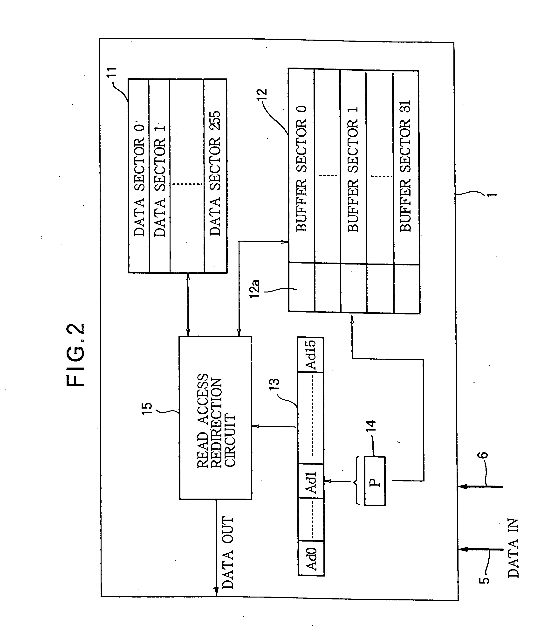
[0130]FIG. 12 is a functional bock diagram of the flash memory unit 1 in the microcomputer in the third embodiment. The flash memory now includes a flash data memory 11 and an erase buffer 16. The flash memory unit 1 also includes an address latch 13, an address pointer 14, and an address RAM 17. The erase buffer 16 and address RAM 17 replace the flash buffer 12 and read access redirection circuit 15 of the first embodiment. The flash data memory 11, address latch 13, and address pointer 14 are equivalent to the corresponding elements in FIG. 2, but are modified with respect to structure and function.

[0131] The flash data memory 11 in the third embodiment has two hundred eighty-eight 34-byte data sectors. Each data sector comprises a 32-byte data area for storing data, and a 2-byte me...


PUM


Abstract

A data storage apparatus includes a flash memory and a control unit that controls the rewriting of data in the flash memory. The flash memory is divided into sectors, each of which is completely erasable in a time T. During a rewriting operation, multiple sectors are erased simultaneously for a time U less than T, and new data are written in a sector that has undergone multiple erasures and is now fully erased. The new data typically replace data stored in a sector that proceeds to be erased during multiple rewriting operations. The duration of each rewriting operation is reduced because the erasing process lasts for time U instead of time T.

Description

CROSS REFERENCE TO RELATED APPLICATIONS [0001] This is a divisional application of application Ser. No. 10 / 665,617, filed Sep. 22, 2003, which is hereby incorporated by reference in its entirety for all purposes.BACKGROUND OF THE INVENTION [0002] 1. Field of the Invention [0003] The present invention relates to a method and apparatus for rewriting data in a flash memory. [0004] 2. Description of the Related Art [0005] Flash memory is a type of electrically erasable programmable read-only memory (EEPROM), in which the rewriting of data involves an erasing process followed by a writing or programming process. The memory cells in a flash memory are organized into small units such as bytes or words, and larger units such as pages or sectors. The erasing process is carried out on one or more pages or sectors at a time, typically by removing electrons from the floating gates of the memory cells; the writing or programming process is carried out one byte or one word at a time, typically by...

Claims


Application Information

Patent Timeline
Patent Type & Authority Applications(United States)
IPC IPC(8): G06F12/00G06F12/02G11C16/10G11C16/02G11C16/16
CPCG11C16/102G11C16/16G11C16/105
Inventor SHONA, YOSHIHIRO
Owner LAPIS SEMICON CO LTD
Why Eureka
Try Eureka