Semiconductor memory device having pre-emphasis signal generator

Active Publication Date: 2006-11-16
SAMSUNG ELECTRONICS CO LTD
View PDF9 Cites 15 Cited by
  • Summary
  • Abstract
  • Description
  • Claims
  • Application Information

AI Technical Summary

Benefits of technology

[0021] The delay control unit may include a mode register set (MRS).
[0022] The secondary output driver may include a PMOS transistor and an NMOS transistor. The PMOS transistor may be connected to a power supply voltage and the NMOS transistor may be connected to a ground voltage. In addition, the PMOS transistor and the NMOS transistor may be commonly connected to the output terminal. The pre-emphasis signal may be applied to a gate electrode of the NMOS transistor such that the pre-emphasis operation is performed on a data signal having a low level.
[0023] According to another exemplary embodiment of the present invention, there is provided a semiconductor memory device which includes a primary output driver, a secondary output driver, and a pre-emphasis signal generator. The pre-emphasis signal generator includes a plurality of auto pulse generators, a plurality of delay circuits, and a delay control unit. The primary output driver outputs a data signal through an output terminal. The secondary output driver is connected to the output terminal and performs a pre-emphasis operation. The pre-emphasis signal generator outputs a pre-emphasis signal to activate the secondary output driver. Each of the plurality of auto pulse generators generate an auto pulse in response to a transition of a corresponding control signal. Each of the plurality of delay circuits receive the auto pulse output from a corresponding one of the auto pulse generators, delays the auto pulse by a predetermined period, and outputs the corresponding pre-emphasis signal. The delay control unit applies each of a plurality of delay control signals to a corresponding one of the delay circuits and controls a delay amou

Problems solved by technology

Another source of noise is signal reflection due to impedance mismatch.
When the signal reflection is large, the inter-symbol interference (ISI) degrades the integrity of the data output signal.
However, when the semiconductor memory device outputs the data signal, skew may be present when the data signal transitions between the low level and the high level due to a differ

Method used


Image

  • Semiconductor memory device having pre-emphasis signal generator
  • Semiconductor memory device having pre-emphasis signal generator
  • Semiconductor memory device having pre-emphasis signal generator

Examples


Embodiment Construction

[0033] Hereinafter, exemplary embodiments of the present invention will be described in detail with reference to the attached drawings. Like reference numerals in the drawings denote like elements.

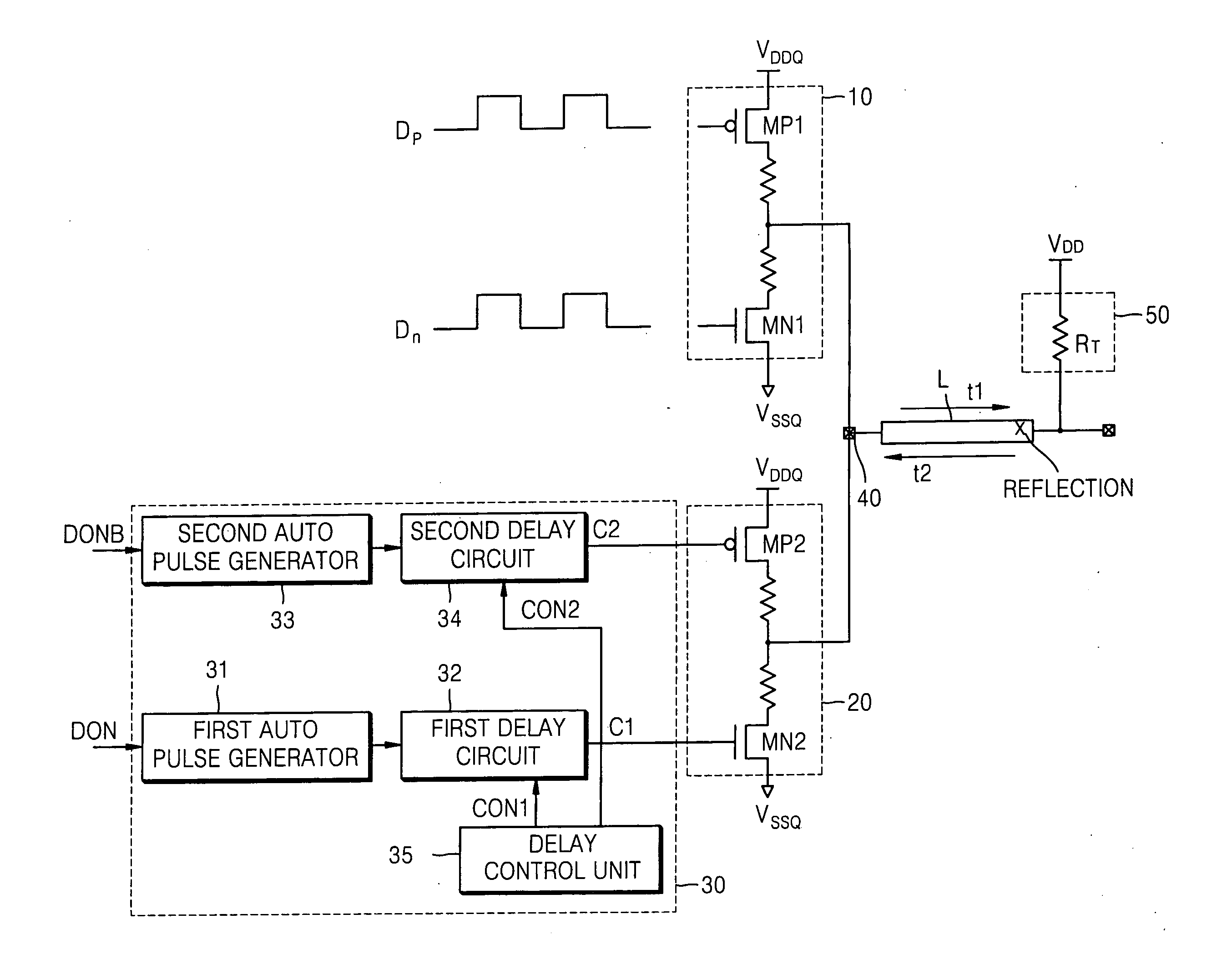
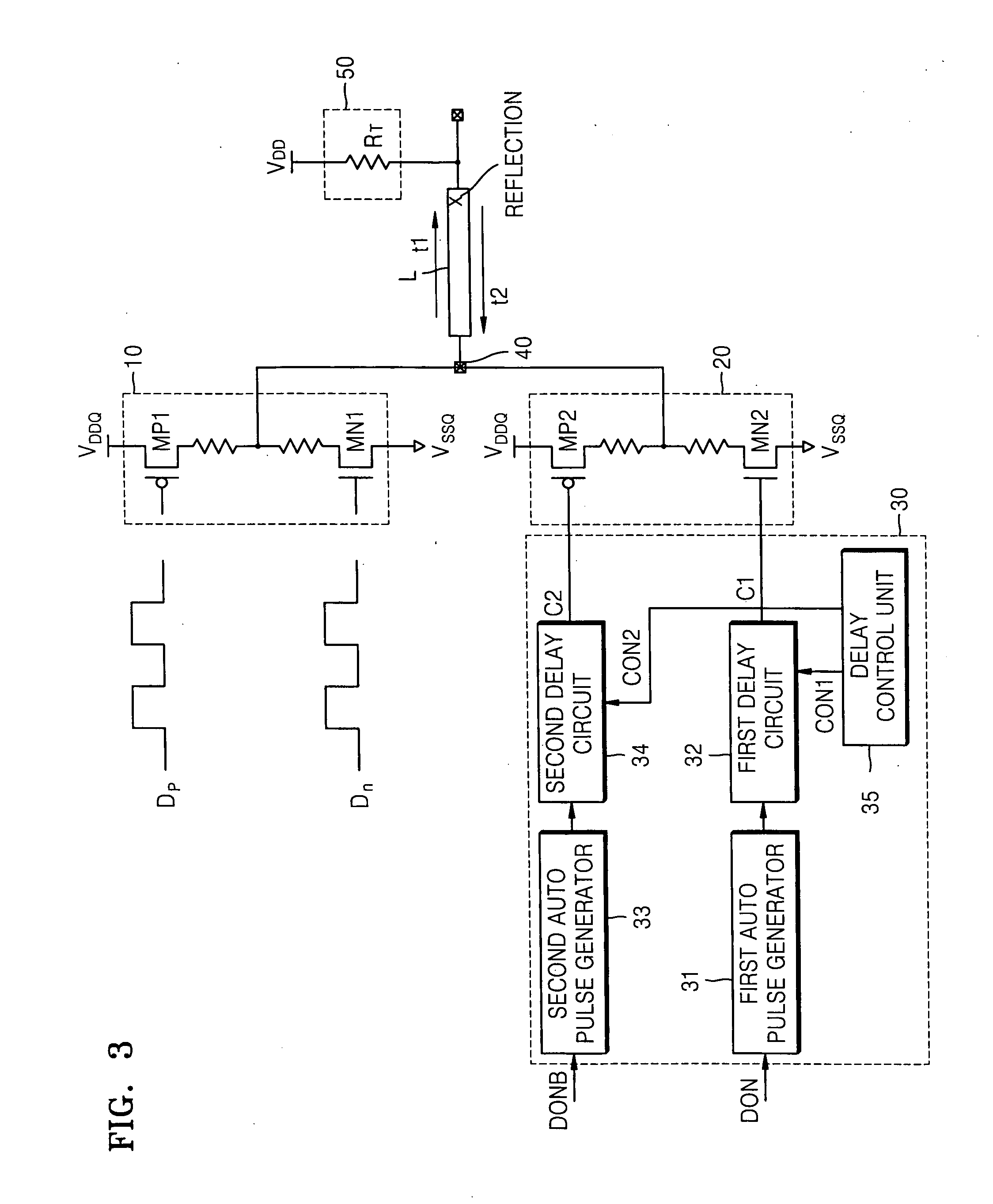
[0034]FIG. 3 illustrates a semiconductor memory device according to an exemplary embodiment of the present invention. For convenience sake, a transmission line L connected to an output terminal 40 of the semiconductor memory device and a termination resistor RT connected to the transmission line L are shown together.

[0035] As shown in FIG. 3, a semiconductor memory device according to an exemplary embodiment of the invention includes a primary output driver 10 for outputting data, and a secondary output driver 20 for performing a pre-emphasis operation. The primary output driver 10 includes a first PMOS transistor MP1 which is electrically connected to a power supply voltage VDDQ and a first NMOS transistor MN1 which is electrically connected to a ground voltage VSSQ. In addition, the fi...


PUM


Abstract

A semiconductor memory device includes a primary output driver which outputs a data signal through an output terminal; a secondary output driver which is connected to the output terminal and performs a pre-emphasis operation; and a pre-emphasis signal generator which outputs a pre-emphasis signal to enable the secondary output driver The pre-emphasis signal generator includes a auto pulse generator which generates an auto pulse in response to a transition of a control signal; a delay circuit which receives the auto pulse output from the auto pulse generator, delays the auto pulse by a predetermined period, and outputs a pre-emphasis signal; and a delay control unit which applies a delay control signal to the delay circuit and controls a delay amount of the delay circuit.

Description

CROSS-REFERENCE TO RELATED PATENT APPLICATION [0001] This application claims priority to Korean Patent Application Nos. 2005-0039717, filed on May 12, 2005 and 2006-0002380, filed on Jan. 9, 2006, in the Korean Intellectual Property Office, the disclosure of which is incorporated by reference herein. BACKGROUND OF THE INVENTION [0002] 1. Field of the Invention [0003] The present invention relates to a semiconductor memory device, and more particularly, to a semiconductor memory device which can efficiently remove noise due to signal reflection. [0004] 2. Description of the Related Art [0005] A semiconductor memory device such as a dynamic random access memory (DRAM) includes an output driver for driving data generated within the memory to another device external to the memory. [0006]FIG. 1 illustrates an output driver of a memory device. As shown in FIG. 1, the output driver includes an inverter 1, a NAND gate 2, a NOR gate 3, a PMOS transistor MP, and an NMOS transistor MN. [0007] ...

Claims


Application Information

Patent Timeline
IPC IPC(8): H03K17/16
CPCG06F13/4072H04L25/028H04L25/0278
Inventor KIM, HYUN-JINPARK, KWANG-ILLEE, WOO-JIN
Owner SAMSUNG ELECTRONICS CO LTD
Why Eureka
Try Eureka