Estimating overlay error and optical aberrations

a technology of optical aberration and overlay error, applied in the field of optical photolithography, can solve the problems of complex processing steps of semiconductor devices, increased complexity, and device performance not good,

Inactive Publication Date: 2006-11-16
MICRON TECH INC
View PDF74 Cites 30 Cited by
  • Summary
  • Abstract
  • Description
  • Claims
  • Application Information

AI Technical Summary

Problems solved by technology

The manufacture and fabrication of semiconductor devices involve complex processing steps.
If the layers are not properly aligned, the device may not perform well, or may even be inoperative.
As semiconductor devices have increased in complexity, the feature dimensions of these devices have decreased, and the influences of optical aberrations become more significant.
Any alignment error produces a displacement of the boxes relative to each other.
Because semiconductor devices are complex and expensive to fabricate, it is desirable to verify registration after the application of each layer.
Registration measurement, verification, and correction can be limited by optical aberrations introduced during the photolithography process.
As discussed earlier, semiconductor devices have increased in complexity.
The feature dimensions of these devices have decreased, and the influences of overlay errors and optical aberrations have become more significant.
However, the accuracy the registration process can be limited by optical aberrations introduced by optical projection element 130 that affect the patterning of wafer

Method used


Image

  • Estimating overlay error and optical aberrations
  • Estimating overlay error and optical aberrations
  • Estimating overlay error and optical aberrations

Examples


Embodiment Construction

[0022] In the following detailed description of the preferred embodiments, reference is made to the accompanying drawings which form a part hereof, and in which is shown by way of illustration specific preferred embodiments in which the inventions may be practiced. These embodiments are described in sufficient detail to enable those skilled in the art to practice the invention, and it is to be understood that other embodiments may be utilized and that logical, mechanical and electrical changes may be made without departing from the spirit and scope of the present invention. The following detailed description is, therefore, not to be taken in a limiting sense, and the scope of the present invention is defined only by the claims.

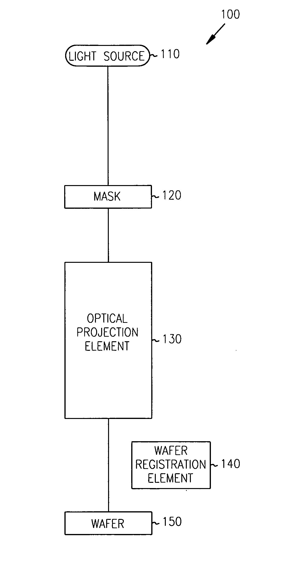
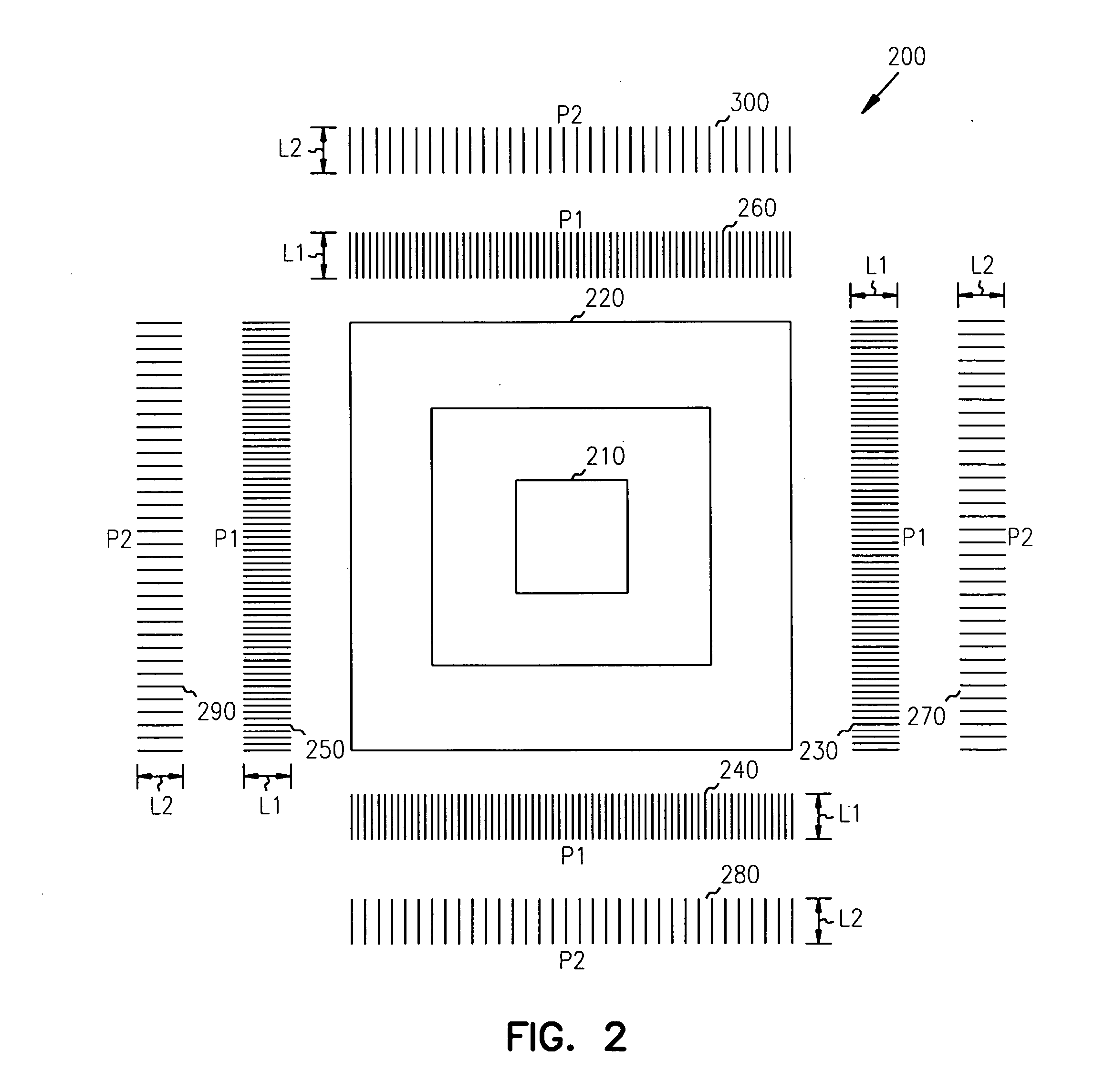
[0023] Some embodiments of the invention provide an aberration mark for use in an optical photolithography system, and a method for estimating overlay errors and optical aberrations. The aberration mark includes an inner polygon pattern and an outer polygon p...


PUM


Abstract

Aberration marks, which may be used in conjunction with lenses in optical photolithography systems, may assist in estimating overlay errors and optical aberrations. Aberration marks may include an inner polygon pattern and an outer polygon pattern, wherein each of the inner and outer polygon patterns include a center, and two sets of lines and spaces having a different feature size and pitch that surround the outer polygon pattern. In some embodiments, the marks can be used with scatterometry or scanning electron microscope devices.

Description

[0001] This application is a Continuation of U.S. application Ser. No. 10 / 889,803, filed Jul. 13, 2004 and incorporated herein by reference.TECHNICAL FIELD [0002] The present disclosure is related to optical photolithography, including the measurement of overlay errors and optical aberrations. BACKGROUND [0003] The manufacture and fabrication of semiconductor devices involve complex processing steps. During the manufacture of integrated circuits, many layers of different materials are applied to a substrate. These layers overlie one another and must be accurately registered to ensure proper operation of the semiconductor device. If the layers are not properly aligned, the device may not perform well, or may even be inoperative. As semiconductor devices have increased in complexity, the feature dimensions of these devices have decreased, and the influences of optical aberrations become more significant. [0004] To aid in the registration of overlying layers in semiconductor devices, r...

Claims


Application Information

Patent Timeline
IPC IPC(8): G01B9/00
CPCG03F7/706G03F7/70641G03F7/70633G03F7/70625
Inventor BOWES, S.W.
Owner MICRON TECH INC
Why Eureka
Try Eureka