Long wave pass infrared filter based on porous semiconductor material and the method of manufacturing the same

a technology of infrared filter and semiconductor material, which is applied in the field of optical filter, can solve the problems of filter type being often strongly limited, filter layers to be delaminate, and filter types can have a number of problems, and achieve the effect of high and flat transmission and improved signal-to-noise ratio of detection system

Inactive Publication Date: 2006-11-16
LAKE SHORE CRYOTRONICS INC
View PDF11 Cites 10 Cited by
  • Summary
  • Abstract
  • Description
  • Claims
  • Application Information

AI Technical Summary

Problems solved by technology

Some optical filters are specialized for different wavelength ranges of light because of limitations in available materials that are optically transparent in the range of interest.
This type of filter is often strongly limited by the width of the flat portion of the transmission band.
In addition, such filters can have a number of problems if used at cryogenic temperatures, a quite common environment for far IR filters serving astronomical and military applications.
This is because thermal stresses during the cooling of the filters can cause layers to delaminate.
This can severely limit the maximum size of the filter, its physical longevity and, through that, the performance and cost-of-use of the optical system incorporating said filters.
However, the mechanical stability of at least some such filters is usually poor since the filtering layer can be easily damaged or removed off the surface of the substrate.
For example, the versions made with thin polymer films cannot withstand pressure differentials (i.e., vacuum pumping) very well.
Such a design will provide higher transmission in the pass band of the filter, but will offer less mechanical stability.

Method used


Image

  • Long wave pass infrared filter based on porous semiconductor material and the method of manufacturing the same
  • Long wave pass infrared filter based on porous semiconductor material and the method of manufacturing the same
  • Long wave pass infrared filter based on porous semiconductor material and the method of manufacturing the same

Examples


Embodiment Construction

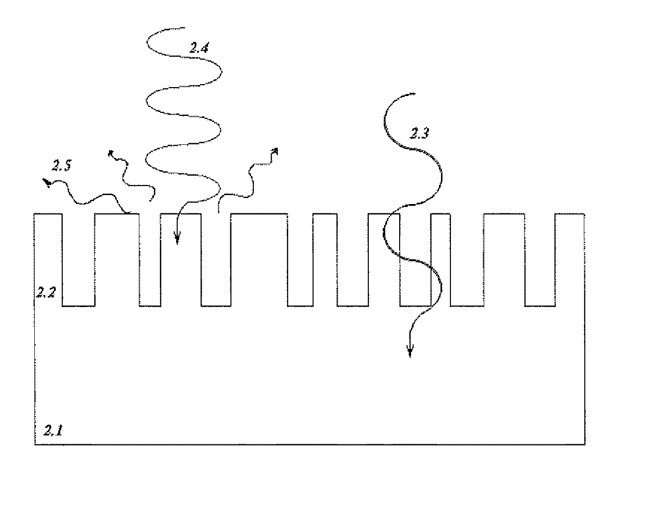
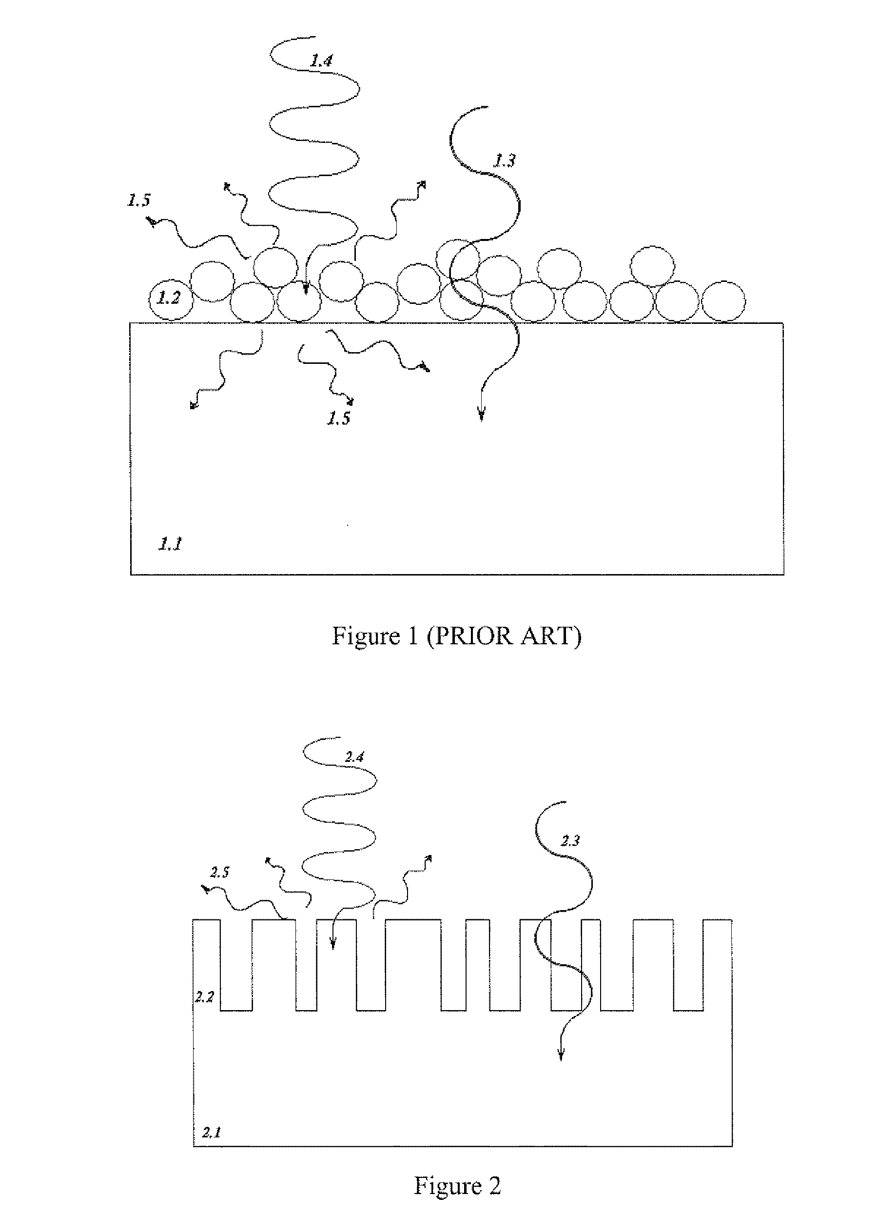
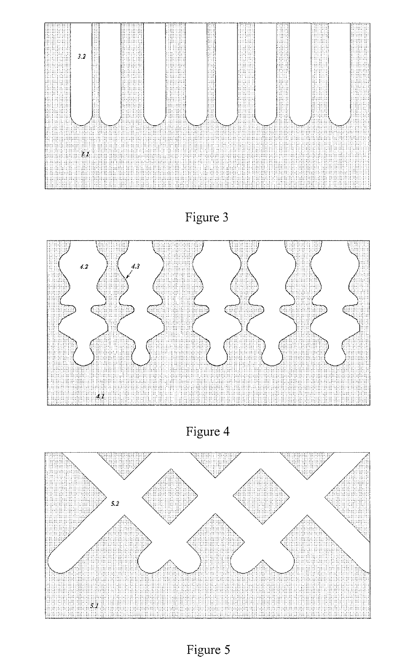
[0037] According to an exemplary non-limiting illustrative implementation, an infrared filter is made of a single-crystal semiconductor wafer having a porous layer etched at least part way through the wafer. Said pores in porous layer are essentially straight and parallel to each other such as illustrated in FIG. 3. For example, such a layer can be electrochemically etched into a silicon wafer with (100) crystallographic orientation (either n- or p-type doped) with resistivity in the range of 0.1 to 1000 Ωcm in HF-containing electrolytes with constant current (galvanostatic) or constant voltage (potentiostatic) anodic etching conditions. Alternatively, an exemplary illustrative non-limiting infrared filter can be fabricated on GaAs, GaP, InP, CaN, Ge or any other semiconductor material wafers that that are known to form the porous layer with straight and parallel pores under electrochemical etching conditions. Backside illumination can be employed during the etching process in order...


PUM


Abstract

Scattering-type long wave pass filters for the infrared region of the spectrum offer high levels of suppression of the unwanted short-wave radiation, good levels of transmission of the desired long wave radiation combined with good control of the rejection edge position and shape and good mechanical stability of the filter layer. Such filters are well suited for the wide range of applications and can be used in various environments including cryogenic temperatures. Several methods of fabrication of such filters based on electrochemical etching of semiconductor materials in order to form porous layer are provided.

Description

CROSS-REFERENCES TO RELATED APPLICATIONS [0001] This application claims the benefit of U.S. Provisional Application No. 60 / 681,155 filed May 16, 2005, entitled “LONG WAVE PASS INFRARED FILTER BASED ON POROUS SEMICONDUCTOR MATERIAL AND THE METHOD OF MANUFACTURING THE SAME” (Attorney Docket 340-99), incorporated herein by reference. [0002] This application is also related to commonly assigned copending application Ser. No. 10 / 686,520 filed 16 Oct. 2003 of Kochergin et al. entitled “SPECTRAL FILTER FOR GREEN AND LONGER WAVELENGTHS” (attorney docket 340-80)STATEMENT REGARDING FEDERALLY SPONSORED RESEARCH OR DEVELOPMENT [0003] Not applicable. FIELD [0004] The technology herein relates to optical filters made of porous semiconductor materials, and more specifically to scattering-type optical filters used in the infrared spectral region. Still more particularly, the technology herein relates to infrared long wave pass filters and band pass filters. [0005] Filters of the exemplary non-limit...

Claims


Application Information

Patent Timeline
Patent Type & Authority Applications(United States)
IPC IPC(8): G06K7/10
CPCG02B5/208G02B5/207
Inventor KOCHERGIN, VLADIMIRSANGHAVI, MAHAVIRMCGOVERN, WILLIAM
Owner LAKE SHORE CRYOTRONICS INC
Why Eureka
Try Eureka