Method of forming a photoresist element

a technology of resist elements and substrate films, applied in the direction of photosensitive materials, photomechanical equipment, instruments, etc., can solve the problems of coating thicknesses that are typically limited to single coating thicknesses, adhesion of coated films to substrate films, and not without problems

Inactive Publication Date: 2006-11-16
MICROCHEM CORP
View PDF32 Cites 116 Cited by
  • Summary
  • Abstract
  • Description
  • Claims
  • Application Information

AI Technical Summary

Benefits of technology

[0019] This invention relates to the preparation of a photoresist element and composite articles of dry film photoresist made using those photoresist elements. Such articles are useful for the fabrication of electronic components, micro-electromechanical system (MEMS) components, micromachine components, microfluidic components, bioMEMS components, micro total analysis system (μ-TAS) components, medical devices, micro optical or waveguide components, microreactor components, electroconductive layers, lithographic galvanoformung abformung (LIGA) components, displays, forms and stamps for microinjection molding and microembossing, screens or stencils for fine printing applications, MEMS and IC packaging (passivation or stress / buffer coats, die attach and no-flow underfills, and the like), wafer level packaging (wafer bonding, chip stacking, 3-D interconnects and the like), integrated passives and printed wiring boards (high density interconnects, solder masks, inner layers, and the like) that can be processed by ultraviolet (UV), x-ray or electron beam lithography. Suitable electronic component applications include dielectric layers, insulation layers, wafer bonding layers and photoconductive wave circuits. Optical applications can include, optical interconnects, waveguides, optical switches, spacers, optical displays, flexible OLEDs, backplanes, diffuser or reflector elements or protective coatings for optical, LED or OLED components. Other uses include as resin or polymer substrates for other photoimageable layers or as films for UV or hot embossing of patterned structures such as for nano-imprint lithography or large area display applications and in the construction of structures for the separation, analysis, and preparation of arrays for biochemical analysis and in the construction of cell growth platforms for biological materials. Still other suitable applications may include the use as cover sheets in the fabrication of buried channel and air-bridge structures used, for example, in microfluidic or optical devices or for the reservoir, fluidic channels or nozzle layer of ink jet heads.

Problems solved by technology

This process is typically limited to single coating thicknesses of 100 μm or less.
While photoresist elements are quite frequently described in the literature, they are not without their problems.
One such problem is the adhesion of the coated film to the substrate film as described in Mimura, U.S. Pat. No. 6,368,722.
Enlow, U.S. Pat. No. 6,254,712, describes the difficulty of extruding polymeric materials into highly transparent, essentially defect-free thin film layers and notes that extrusion techniques have not been successfully adapted to producing high optical quality films at high line speeds and at low cost.
The make-coat layer is then applied to appropriate backing materials via lamination that would normally present processing problems.

Method used


Image

  • Method of forming a photoresist element

Examples


example 1

Formulation of Dry Film Coating Composition Using Hot Melt Processing

[0069] A dry film photoresist coating composition was made by combining the components in Table 1 as shown below.

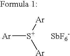
TABLE 1Formulary of the dry film photoresist coating composition of Example 1.WeightWeight %Weight %MaterialTypeSuppliergramson A + D + Fof CompSU-8 ResinResin AResolution Performance145.072.567.1ProductsNC-3000HResin ANippon Kayaku Co., Ltd.40.020.018.5ResinHeloxyReactiveResolution Performance12.06.05.6Modifier 48Monomer DProductsZ6040 SilaneAdhesionDow Corning Company3.01.51.4Promoter FCyracure 6974*PAG BDow Chemical Company16.08.07.4Total216.0100

*Cyracure 6974 contains a nominal 50.0 weight % of aryl sulphonium hexafluoroantimonate salts in propylene carbonate solvent.

[0070] A 250 ml beaker containing a magnetic stirrer and wrapped with a heating tape was placed on a magnetic stirrer hot plate. To this was added the Reactive Monomer D and the Adhesion Promoter F. This was heated to approximately 1...

examples 2-6

Dry Film Photoresist Compositions were Made by Combining the Components as Shown in Table 2

[0072]

TABLE 2Formulary of the dry film photoresist coating compositions of Examples 2-6.Example 2Example 3Example 4Example 5Example 6Weight,Weight,Weight,Weight,Weight,gmsgmsgmsgmsgms(% on(% on(% on(% on(% onMaterialTypeSupplierA + D + F)A + D + F)A + D + F)A + D + F)A + D + F)SU-8 ResinResin AResolution137.0137.0137.0137.0137.0Performance(68.5)(68.5)(68.5)(68.5)(68.5)ProductsNC-3000H ResinResin ANippon Kayaku50.0—50.050.050.0Co., Ltd.(25.0)(25.0)(25.0)(25.0)NER-7604 ResinResin ANippon Kayaku—50.0———Co., Ltd.(25.0)Heloxy Modifier 48ReactiveResolution10.010.013.013.013.0Monomer DPerformance(5.0)(5.0)(6.5)(6.5)(6.5)ProductsZ6040 SilaneAdhesionDow Corning3.03.0———Promoter FCompany(1.5)(1.5)Cyracure 6974*PAG BDow Chemical———8.0—Company(4.0)OPPIPAG BHampford8.08.08.0——Research(4.0)(4.0)(4.0)ProductsCD-1012PAG BSartomer————8.0(4.0)2-Ethoxy-8,9-Sensitizer EHampford0.120.120.12—0.12dimethoxyResearch(0...

examples 7-9

Dry film Photoresist Compositions were Made by Combining the Components as Shown in Table 3

[0074]

TABLE 3Formulary of the dry film photoresist coating compositions of Examples 7-9.Example 7Example 8Example 9Weight, gmsWeight, gmsWeight, gmsMaterialTypeSupplier(% on A + D + F)(% on A + D + F)(% on A + D + F)SU-8 ResinResin AResolution685.0685.0267.5Performance(68.5)(68.5)(53.5)ProductsNC-3000H ResinResin ANippon Kayaku250.0250.0125.0Co., Ltd.(25.0)(25.0)(25.0)NER-7604 ResinResin ANippon Kayaku——75.0Co., Ltd.(15.0)Heloxy Modifier 48ReactiveResolution65.065.032.5Monomer DPerformance(6.5)(6.5)(6.5)ProductsZ6040 SilaneAdhesionDow Corning———Promoter FCompanyCyracure 6974*PAG BDow Chemical—80.0—Company(8.0)OPPIPAG BHampford———ResearchProductsCD-1012PAG BSartomer40.0——(4.0)2-Ethoxy-8,9-Sensitizer EHampford0.60——dimethoxyResearch(0.06)anthraceneProductsTotal1040.61080.0500.0

*Cyracure 6974 contains a nominal 50.0 weight % of aryl sulphonium hexafluoroantimonate salts in propylene carbonate sol...


PUM

PropertyMeasurementUnit
equivalent weightaaaaaaaaaa
particle sizeaaaaaaaaaa

Abstract

A method of forming a photoresist element comprising the steps of: preparing a hot melt photoresist mixture; applying the photoimageable hot melt composition to a film substrate using a slot die coating system; cooling the hot melt sufficiently to prevent flow; and applying a protective cover film to the opposite surface of the partially cooled composition, thereby forming a photoresist element.

Description

CROSS-REFERENCE TO RELATED APPLICATIONS [0001] This application claims the benefit of U.S. Provisional Patent Application No. 60 / 680,801 filed May 13, 2005.BACKGROUND OF THE INVENTION [0002] 1. Field of the Invention [0003] This invention relates to a method of forming a photoresist element using a slot die coating system. The present invention also relates to composite articles of manufacture made using the photoresist element. [0004] 2. Brief Description of Art [0005] Photoimageable coatings (commonly known as photoresists) are currently used in a wide variety of semiconductor and micromachining applications. In such applications, photoimaging is accomplished by exposing a photosensitive coating on a substrate to patterned radiation thereby inducing a solubility change in the coating such that the exposed or unexposed regions can be selectively removed by treatment with a suitable developer composition. The photoimageable coating or photoresist may be either of the positive or neg...

Claims


Application Information

Patent Timeline
Patent Type & Authority Applications(United States)
IPC IPC(8): G03C1/00
CPCG03F7/038G03F7/161G03F7/0385G03C1/76G03F7/11B82B3/00
Inventor JOHNSON, DONALD W.
Owner MICROCHEM CORP
Why Eureka
Try Eureka