Manufacturing method for semiconductor wafers, slicing method for slicing work and wire saw used for the same

US20060258268A1Inactive Publication Date: 2006-11-16KOMATSU NTC LTD +1

Image

  • Manufacturing method for semiconductor wafers, slicing method for slicing work and wire saw used for the same
  • Manufacturing method for semiconductor wafers, slicing method for slicing work and wire saw used for the same
  • Manufacturing method for semiconductor wafers, slicing method for slicing work and wire saw used for the same

Examples


Embodiment Construction

[0092] An embodiment of the present invention will be described in detail with reference to the accompanying drawings.

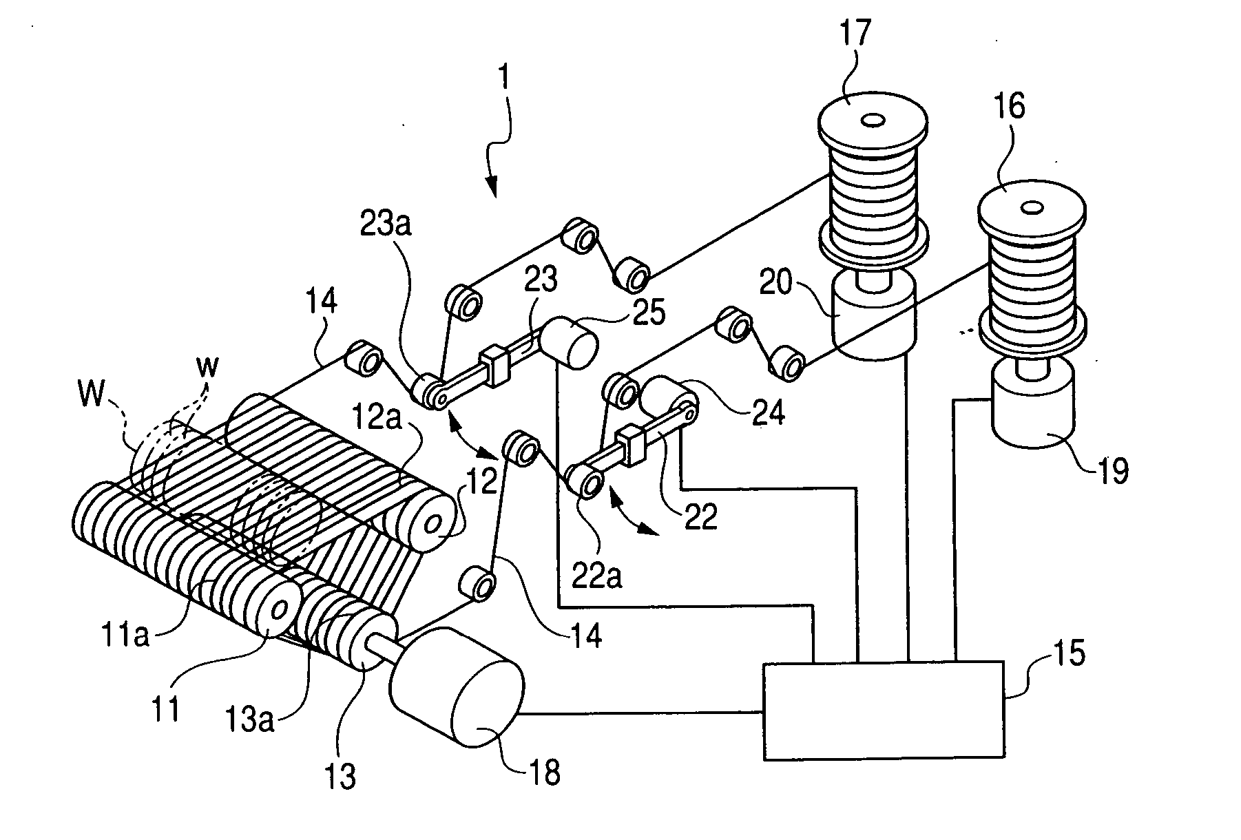
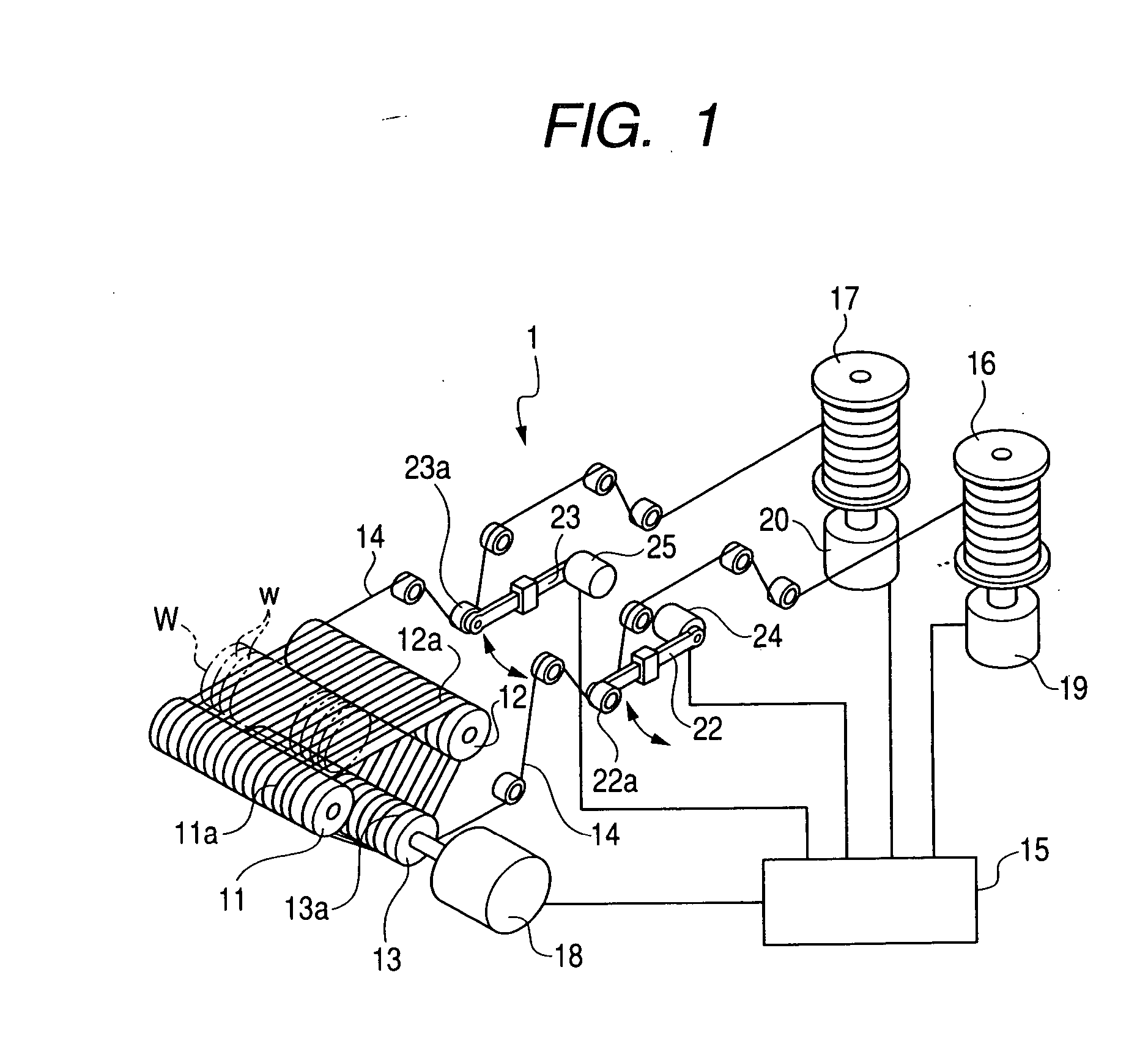
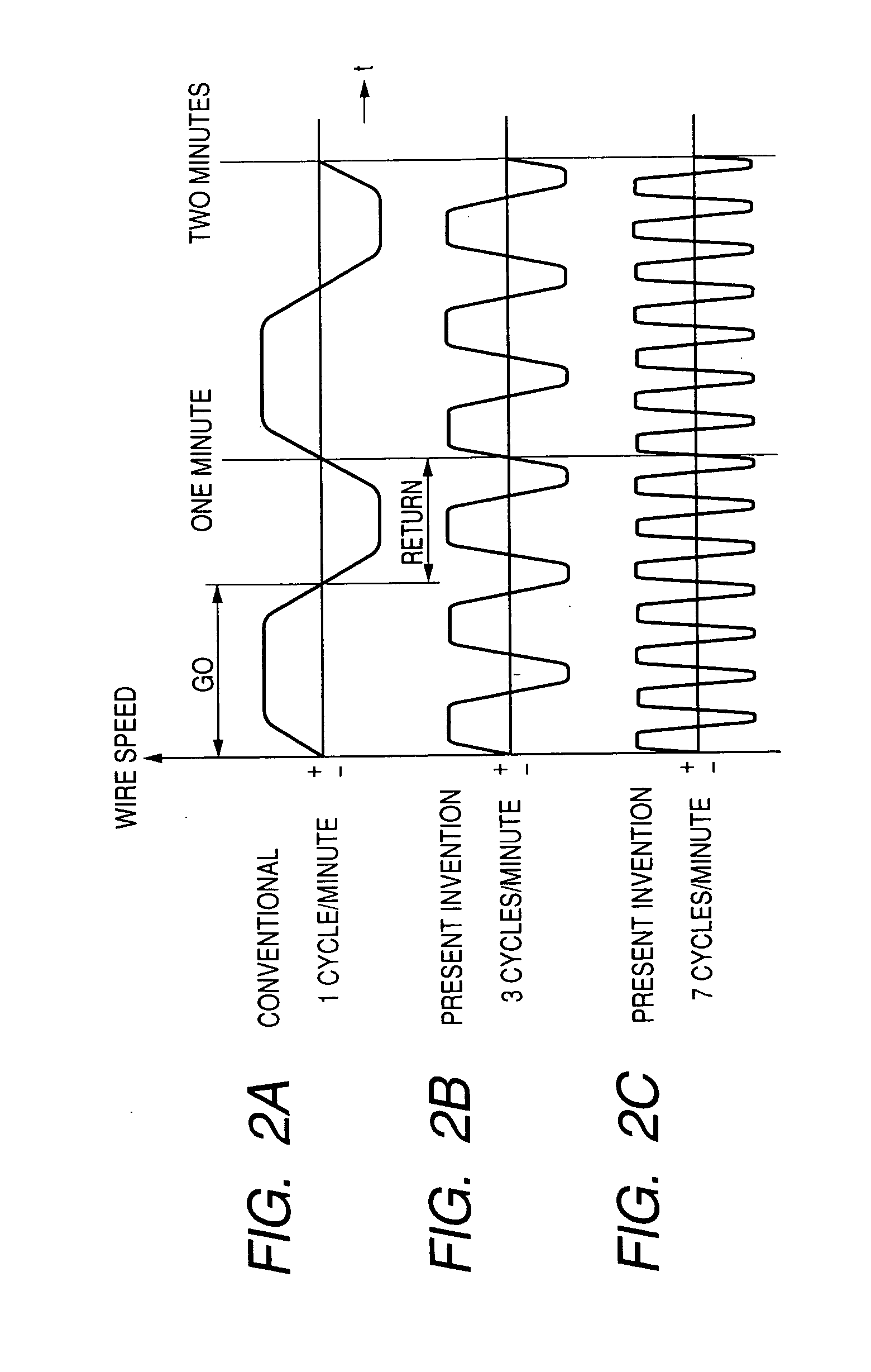
[0093] After a detailed study and many experiments, inventors confirmed that in a wire saw as shown in FIG. 1, long period waviness on a wafer surface disappears after slicing a work by reciprocating a wire of 3 or more and less than 8 reciprocations per a minute. First, the wire saw will be described.

[0094]FIG. 1 is a perspective view illustrating a main part of the wire saw. As shown in FIG. 1, the wire saw 1 includes three processing rollers 11, 12 and 13 disposed at predetermined intervals thereamong. A plurality of annular grooves are formed at outer peripherals of the respective processing rollers 11, 12 and 13 with predetermined pitches. Also, one wire 14 has both ends wound around a pair of reels 16 and 17, respectively. In addition, between both reels 16 and 17, the wire 14 is wound continuously around the annular grooves 11a, 12a and 13a of the respective...


PUM

PropertyMeasurementUnit
Poweraaaaaaaaaa
Poweraaaaaaaaaa
Lengthaaaaaaaaaa

Abstract

In order to omit a lapping process or a double disk grinding process by performing slicing operation so as not to generate long period waviness on the surface of the wafer in a slicing process and by completely removing short period waviness remaining in the surface of the sliced wafer during a polishing process, there is provided a manufacturing method includes a slicing process of slicing a work of the semiconductor wafer by reciprocating a wire of a wire saw at constant cycles of 3 or more and less than 8 per a minute a grinding process of grinding both sides of the sliced wafer by a grinding wheel, one-side by one-side and a polishing process of performing a chemical mechanical polishing on both sides of the ground wafer by a fixed abrasive grain polishing cloth, in which an abrasive grain is fixed, and a abrasive containing no abrasive grains.

Description

[0001] The present invention claims foreign priority to Japanese patent application No. P.2005-125989, filed on Apr. 25, 2005, the contents of which is incorporated herein by reference. BACKGROUND OF THE INVENTION [0002] 1. Field of the Invention [0003] The present invention relates to a manufacturing method for semiconductor wafers, a slicing method of slicing a work, and a wire saw used for the same. [0004] 2. Description of the Background Art [0005] Conventionally, semiconductor wafers (hereinafter, called wafers) has been manufactured according to a manufacturing process shown in a flowchart of FIG. 10. As shown in FIG. 10, the first step S202 is a slicing process. That is, in step S202, an outer peripheral of a single crystal ingot, which is manufactured by, for example, a single crystal pulling method, is ground, and then, an orientation flat process, a notch process or the like is performed so as to determine a position of a crystalline orientation, after that, the single cry...

Claims


Application Information

Patent Timeline
16 Nov 2006
Publication
US20060258268A1
IPC
B24B1/00; B28D1/08; B24B7/30; B24B9/00; B24B7/20; B24B27/06; B24B37/04; B24D3/28; B24D11/00; B28D5/04; H01L21/304
CPC
B28D5/045; B23D57/0053; H01L21/30
Inventors
MIYATA, KENSYO; HARADA, SEIJI