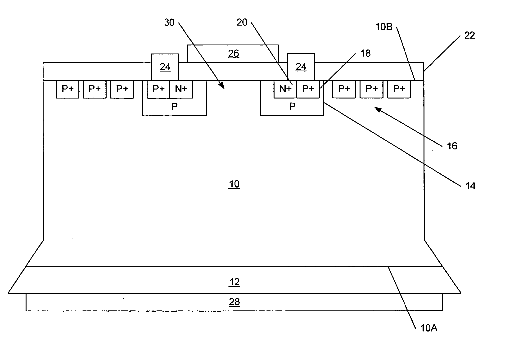
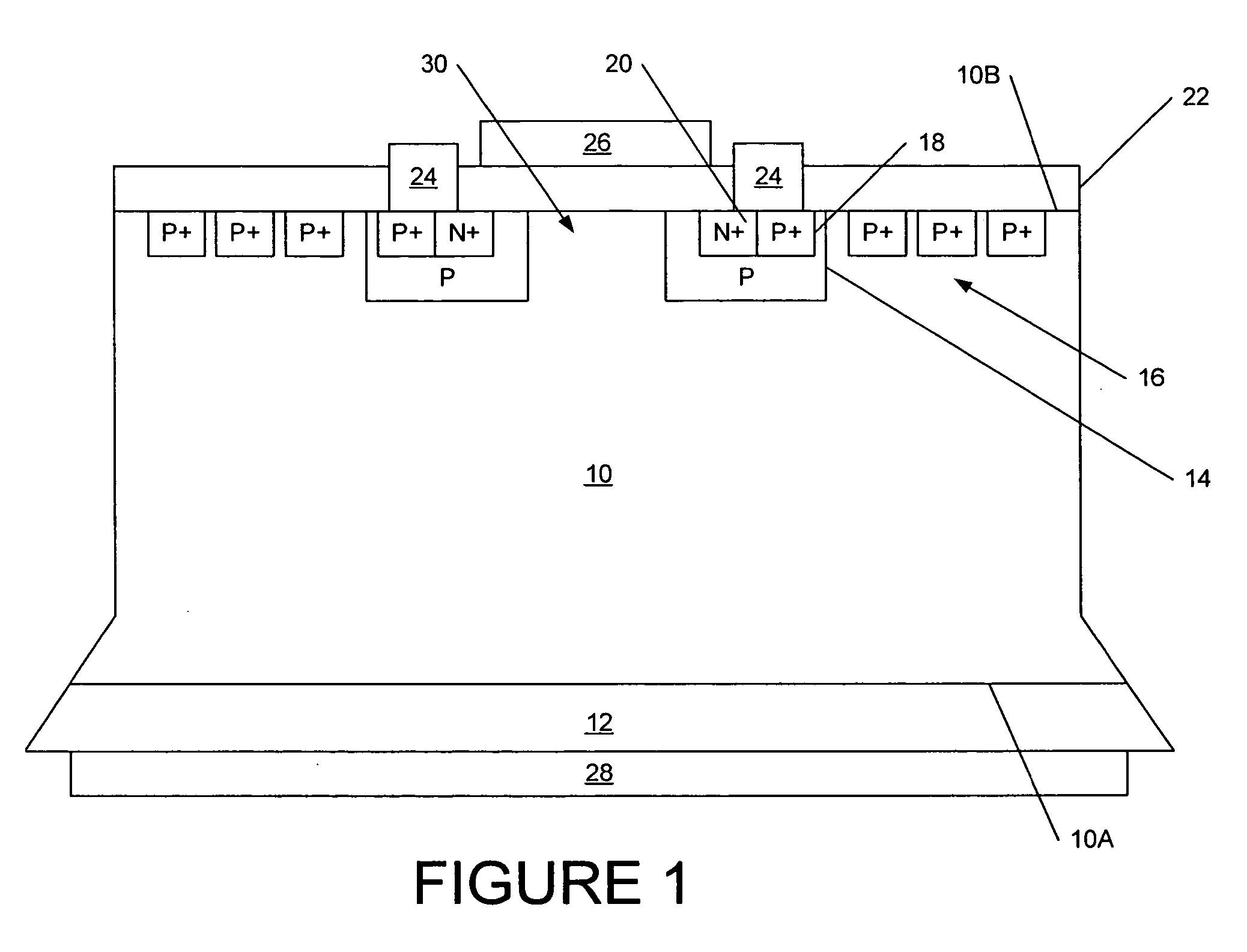
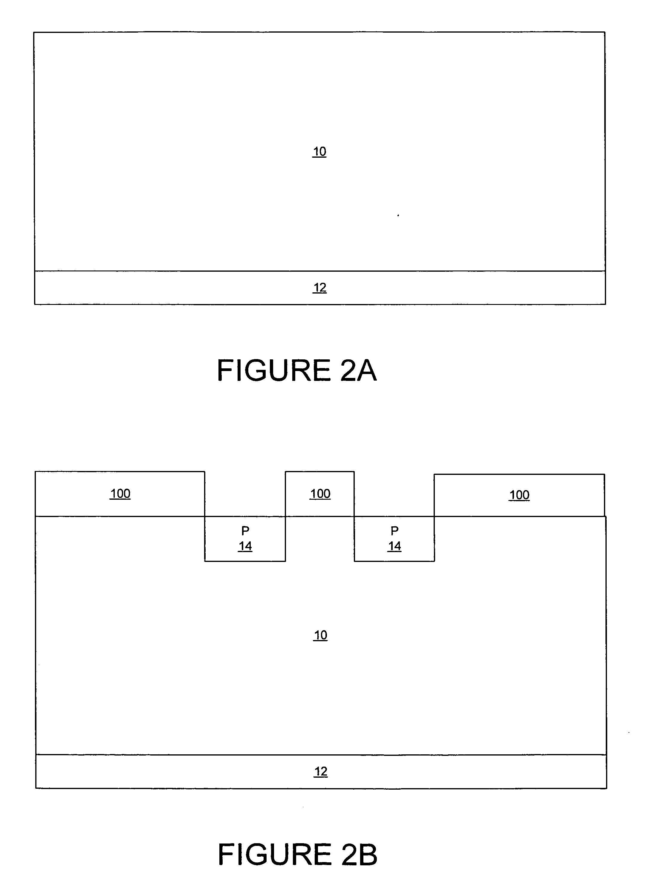
High voltage silicon carbide MOS-bipolar devices having bi-directional blocking capabilities and methods of fabricating the same

a technology of silicon carbide and bipolar transistors, applied in the direction of semiconductor devices, electrical apparatus, transistors, etc., can solve the problems of bipolar transistors being vulnerable to premature breakdown, bipolar transistors being relatively difficult to operate in parallel, and complex base drive circuitry for controlling turn-on and turn-o

Active Publication Date: 2006-11-23
CREE INC
View PDF8 Cites 50 Cited by
  • Summary
  • Abstract
  • Description
  • Claims
  • Application Information

AI Technical Summary

Benefits of technology

[0023] While the present invention is described above primarily with reference to high voltage devices and IGBTs, methods of fabricating high voltage devices and IGBTs are also provided herein.

Problems solved by technology

Despite the attractive power ratings achieved by bipolar transistors, there exist several fundamental drawbacks to their suitability for all high power applications.
Because of the large base current demands, the base drive circuitry for controlling turn-on and turn-off is relatively complex and expensive.
Bipolar transistors may also be vulnerable to premature breakdown if a high current and high voltage are simultaneously applied to the device, as commonly required in inductive power circuit applications.
Furthermore, it may be relatively difficult to operate bipolar transistors in parallel because current diversion to a single transistor typically occurs at high temperatures, making emitter ballasting schemes necessary.
This current diversion generally results from the decrease in on-state voltage drop across the bipolar device with further increases in operating temperature.
Notwithstanding the potential advantages of silicon carbide, it may be difficult to fabricate power devices, including IGBTs, in silicon carbide.
Low resistivity p-type silicon carbide substrates may not be available as a result of the available acceptor species (Aluminum and Boron) having deep energy levels that may result in carrier freeze out.
Thus, the exclusive use of n-type substrates may limit the polarity of available high voltage devices.
In addition, the available devices may only be capable of blocking voltages in one direction.
As is noted above, highly doped p-type substrates currently are more difficult to fabricate than n-type substrates in silicon carbide.
Thus, present silicon carbide IGBTs may require more complex gate drive circuitry with level shifting components and result in more complex power circuits as a result of the structure of IGBTs, the electrical characteristics of silicon carbide and the limitations in fabrication of highly doped p-type silicon carbide substrates.
Forming planar edge termination structures on a backside of the device may be difficult and costly to implement as extensive processing may be needed after removal of the 300 to 400 μm thick n-type substrate.
Edge beveling may include etching through the substrate or grinding / polishing the sidewalls of the device, which may also be difficult because the voltage blocking epitaxial layers are generally much thinner than the substrate.

Method used


Image

  • High voltage silicon carbide MOS-bipolar devices having bi-directional blocking capabilities and methods of fabricating the same
  • High voltage silicon carbide MOS-bipolar devices having bi-directional blocking capabilities and methods of fabricating the same
  • High voltage silicon carbide MOS-bipolar devices having bi-directional blocking capabilities and methods of fabricating the same

Examples


Embodiment Construction

[0026] The present invention now will be described more fully hereinafter with reference to the accompanying drawings, in which embodiments of the invention are shown. This invention may, however, be embodied in many different forms and should not be construed as limited to the embodiments set forth herein. Rather, these embodiments are provided so that this disclosure will be thorough and complete, and will fully convey the scope of the invention to those skilled in the art. In the drawings, the size and relative sizes of layers and regions may be exaggerated for clarity. It will be understood that when an element or layer is referred to as being “on”, “connected to” or “coupled to” another element or layer, it can be directly on, connected or coupled to the other element or layer or intervening elements or layers may be present. In contrast, when an element is referred to as being “directly on,”“directly connected to” or “directly coupled to” another element or layer, there are no...


PUM


Abstract

Silicon carbide high voltage semiconductor devices and methods of fabricating such devices are provided. The devices include a voltage blocking substrate. Insulated gate bipolar transistors are provided that have a voltage blocking substrate. Planar and beveled edge termination may be provided.

Description

FIELD OF THE INVENTION [0001] This invention relates to power semiconductor devices and related methods of fabricating power semiconductor devices and, more particularly, to high voltage silicon carbide devices and related methods of fabricating high voltage silicon carbide devices. BACKGROUND OF THE INVENTION [0002] Power devices are widely used to carry large currents and support high voltages. Modern power devices are generally fabricated from monocrystalline silicon semiconductor material. One type of power device is the thyristor. A thyristor is a bistable power semiconductor device that can be switched from an off-state to an on-state, or vice versa. Power semiconductor devices, such as thyristors, high-power bipolar junction transistors (“HPBJT”), or power metal oxide semiconductor field effect transistors (“MOSFET”), are semiconductor devices capable of controlling or passing large amounts of current and blocking high voltages. [0003] Silicon bipolar transistors have, conven...

Claims


Application Information

Patent Timeline
Patent Type & Authority Applications(United States)
IPC IPC(8): H01L29/15
CPCH01L29/1608H01L29/7395H01L29/66333H01L29/66068
Inventor RYU, SEI-HYUNGJENNY, JASON R.DAS, MRINAL K.HOBGOOD, HUDSON MCDONALDAGARWAL, ANANT K.PALMOUR, JOHN W.
Owner CREE INC
Why Eureka
Try Eureka