Nanotube Schottky diodes for high-frequency applications

Inactive Publication Date: 2006-11-23
CALIFORNIA INST OF TECH
View PDF4 Cites 53 Cited by
  • Summary
  • Abstract
  • Description
  • Claims
  • Application Information

AI Technical Summary

Benefits of technology

[0008] In one aspect, the first conductive contact is formed of a material that has a lower work function than that of the nanotube to form a Schottky

Problems solved by technology

However, above a few hundred GHz, the inherent parasitic capacitance (proportional to semiconductor junction area) and resistance (inversely proportional to electron mobility) of these devices severely limit the achievable sensitivity for detection, (direct detector noise equivalent power (NEP)˜10−12 W/square-root (√) Hz, heterodyne N

Method used


Image

  • Nanotube Schottky diodes for high-frequency applications
  • Nanotube Schottky diodes for high-frequency applications
  • Nanotube Schottky diodes for high-frequency applications

Examples


Embodiment Construction

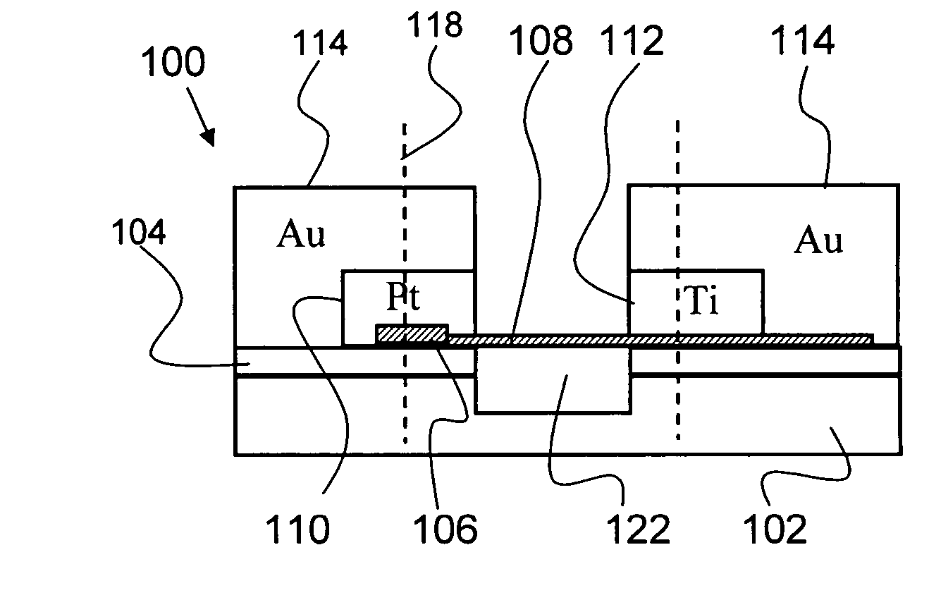
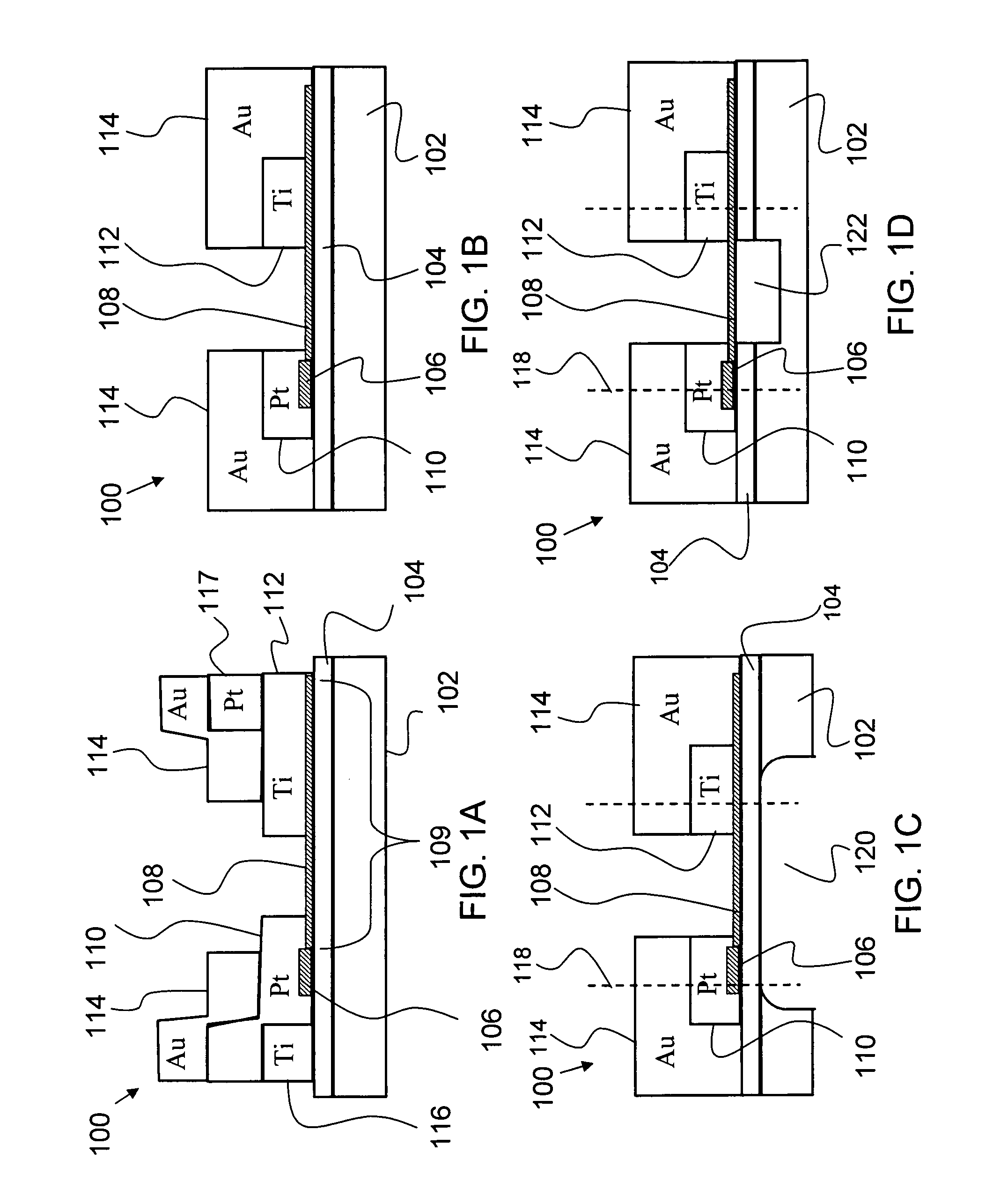
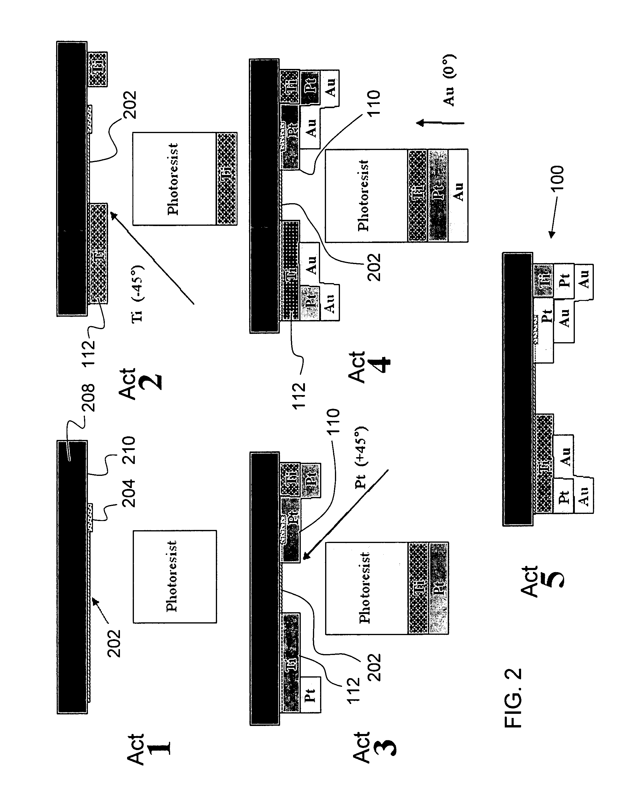
[0027] The present invention relates to Schottky diodes and, more particularly, to Schottky diodes using semi-conducting single-walled nanotubes (s-SWNTs) with dissimilar contacts (e.g., a titanium Schottky contact and a platinum Ohmic contact) for high-frequency applications. The following description is presented to enable one of ordinary skill in the art to make and use the invention and to incorporate it in the context of particular applications. Various modifications, as well as a variety of uses in different applications will be readily apparent to those skilled in the art and the general principles defined herein may be applied to a wide range of embodiments. Thus, the present invention is not intended to be limited to the embodiments presented, but is to be accorded the widest scope consistent with the principles and novel features disclosed herein.

[0028] In the following detailed description, numerous specific details are set forth in order to provide a more thorough under...


PUM


Abstract

Described is a Schottky diode using semi-conducting single-walled nanotubes (s-SWNTs) with titanium Schottky and platinum Ohmic contacts for high-frequency applications. The diodes are fabricated using angled evaporation of dissimilar metal contacts over an s-SWNT. The devices demonstrate rectifying behavior with large reverse-bias breakdown voltages of greater than −15 V. In order to decrease the series resistance, multiple SWNTs are grown in parallel in a single device, and the metallic tubes are burnt-out selectively. At low biases, these diodes showed ideality factors in the range of 1.5 to 1.9. Modeling of these diodes as direct detectors at room temperature at 2.5 terahertz (THz) frequency indicates noise equivalent powers (NEP) comparable to that of the state-of-the-art gallium arsenide sold-state Schottky diodes, in the range of 10-13 W/square-root (√) Hz.

Description

PRIORITY CLAIM [0001] The present application is a non-provisional application, claiming the benefit of U.S. Provisional Application No. 60 / 683,825, filed on May 23, 2005, titled, “Carbon Nanotube Schottky Diodes for High Frequency Applications.”GOVERNMENT RIGHTS [0002] The invention described herein was made in the performance of work under a NASA contract and is subject to the provisions of Public Law 96-517 (35 USC 202) in which the Contractor has elected to retain title.FIELD OF INVENTION [0003] The present invention relates to Schottky diodes, and more particularly, to Schottky diodes using semi-conducting single-walled nanotubes (s-SWNTs) with dissimilar contacts for high-frequency applications. BACKGROUND OF INVENTION [0004] For high-frequency applications in the range of 30 gigahertz (GHz) to 3 terahertz (THz), (i.e., microwave to sub-millimeter wave region), diodes are of particular interest as detectors, mixers, and frequency multipliers. In particular, solid-state Schottk...

Claims


Application Information

Patent Timeline
IPC IPC(8): H01L21/00
CPCB82Y10/00H01L29/0665H01L29/872H01L29/66143H01L29/0673
Inventor MANOHARA, HARISHHUNT, BRIANSCHLECHT, ERICHSIEGEL, PETERWONG, ERIC
Owner CALIFORNIA INST OF TECH
Why Eureka
Try Eureka