Optical information recording medium, and information recording method and information reproducing method using the same
a technology of information recording and information, applied in the field of large-capacity optical disk technology, can solve the problems of difficult to record a minute mark with excellent reproducibility, and achieve the effect of increasing the density of recording data and excellent reproducibility
- Summary
- Abstract
- Description
- Claims
- Application Information
AI Technical Summary
Benefits of technology
Problems solved by technology
Method used
Image
Examples
first embodiment
[0077] A case describes that the present invention is achieved by using Ag and Fe as a recording film. An optical disk having a structure shown in FIG. 5A was fabricated. All thin films were deposited by a sputtering technique. A 200 nm thick Ag film 507, a 5 nm thick SiO2 film 506, a 5 nm thick amorphous state Ge2Sb2Te5 film 505, a 5 nm thick Cr2O3 film 504, a 110 nm thick SiO2 film 503, a 5 nm thick Cr2O3 film 502, and a 0.1 nm thick polycarbonate sheet were stacked on a glass substrate 508. Next, as shown in FIG. 5B, the phase change film 505 which is in a state close to an amorphous one is crystallized by irradiating a laser beam to make a crystallized phase change film 509. Next, a laser beam is irradiated to this optical disk and the recording film is locally molten to record an amorphous mark 510 as shown in FIG. 5C.
[0078]FIG. 6 is an example of a configuration illustrating the recording device. This device is also equipped with the ability to reproduce the mark, and the con...
second embodiment
[0095] Here, a case where a chevron type pattern pit is formed is described. An amorphous mark was recorded by using the device shown in FIG. 6 on the phase change film of the optical disk having a structure shown in FIG. 5A, which is the same as the first embodiment. However, here, Ge5Sb70Te25 was used for the phase change film, not Ge2Sb2Te5. This phase change film makes it possible to form a chevron mark such as the one described in the Japanese Journal of Applied Physics, Vol. 41, pp. 631-635. The recording conditions were a disk line speed of 2 m / s, a track pitch of 240 nm, and the recording waveform was the one shown in FIG. 11. Accordingly, a chevron type amorphous mark with a mark length of 20 nm and a space length of 20 nm could be recorded.
[0096] A pattern pit was formed by peeling off and etching this optical disk as shown in FIGS. 5D and 5E. A mold of a pattern pit could be taken in the UV resin by applying this optical disk to a sample on which the UV resin was coated ...
third embodiment
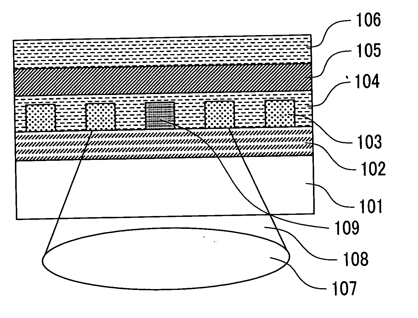
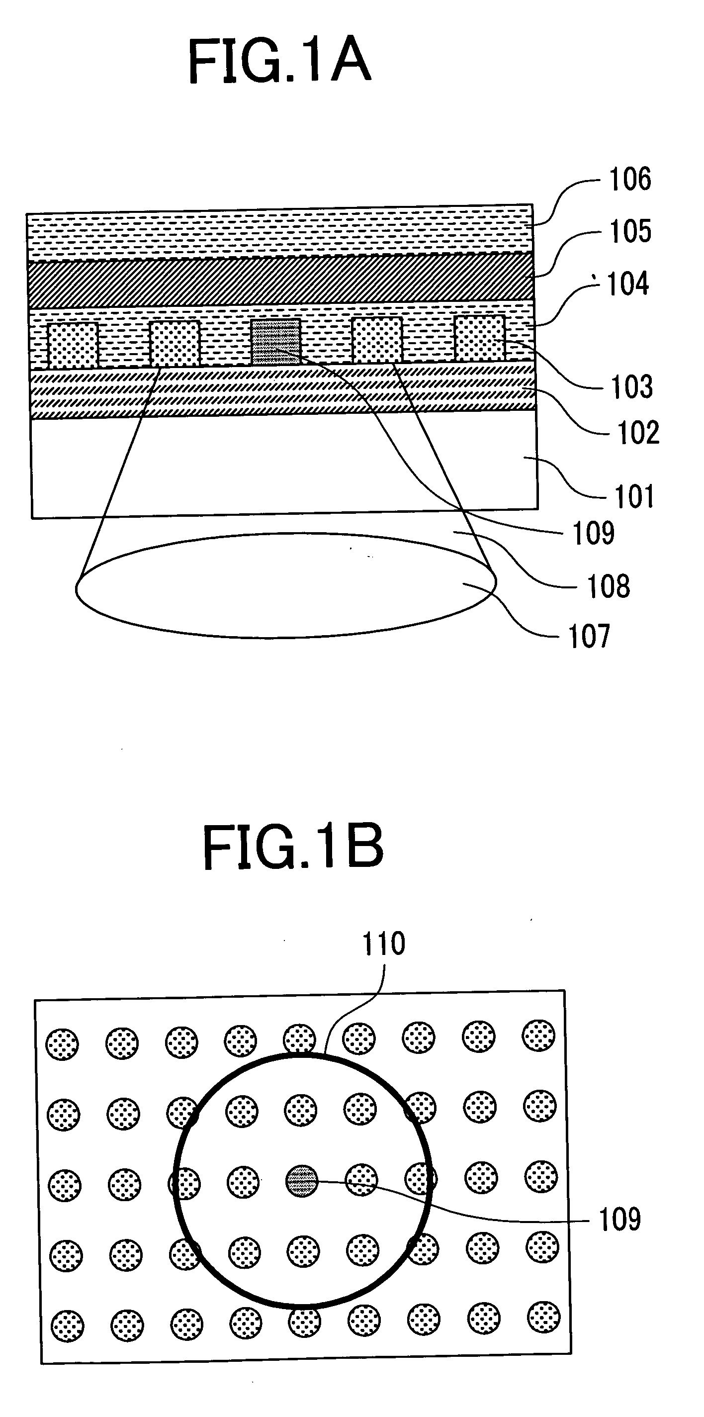
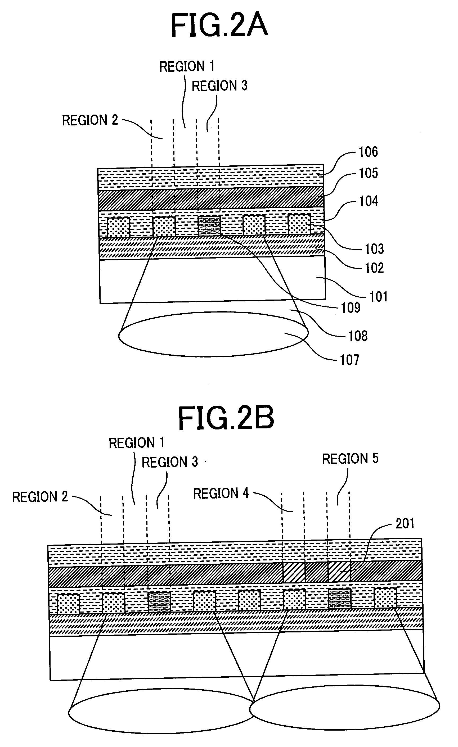
[0099] A case where Si and Cr are used for a recording film is described. A stamper was fabricated by a method shown in the second embodiment. A pattern of the stamper was transferred to the optical disk having the following structure formed by sputtering in the same manner as the second embodiment: 0.1 mm thick polycarbonate sheet / SiO2 (50 nm) / Cr2O3 (5 nm) / Ge5Sb70Te25 (5 nm). After transfer, etching was performed under the same conditions as the first embodiment to make it the state of FIG. 4D. Films as follows were deposited on this sample: Cr2O3 (5 nm) / SiO2 (20 nm) / Si (10 nm) / Cr (10 nm) / SiO2 (110 nm) / Ag (30 nm). A 1.1 mm thick polycarbonate substrate was affixed on the Ag film of this disk using a UV curable resin to fabricate an optical disk. The optical characteristics of this optical disk are shown in Table 2.
TABLE 2Region 1Region 2Region 3Region 4Region 5State ofNot existNot existNot existExistExistrecordingmarkState ofNot existCrystallineMoltenCrystallineMoltenpattern pitR...
PUM
| Property | Measurement | Unit |
|---|---|---|
| diameter | aaaaa | aaaaa |
| diameter | aaaaa | aaaaa |
| melting point | aaaaa | aaaaa |
Abstract
Description
Claims
Application Information


