
Method for forming material layer between liquid and photoresist layer

a technology of liquid and lithography, applied in the field of forming a material layer, can solve the problems of lithography defects, certain technical problems still exist, etc., and achieve the effect of avoiding the reaction between the photoresist and the liquid

Inactive Publication Date: 2006-11-23
UNITED MICROELECTRONICS CORP
View PDF5 Cites 0 Cited by
  • Summary
  • Abstract
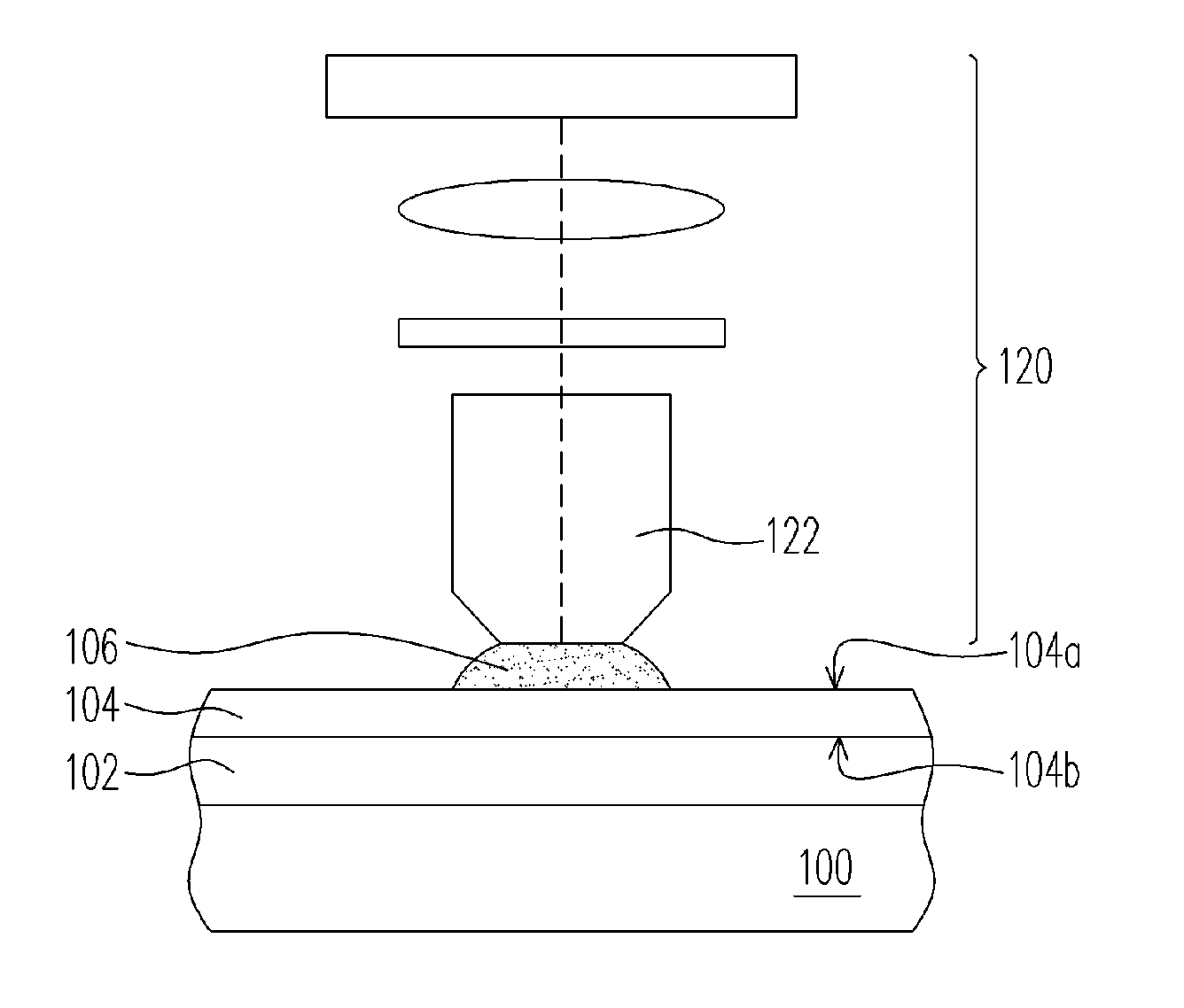
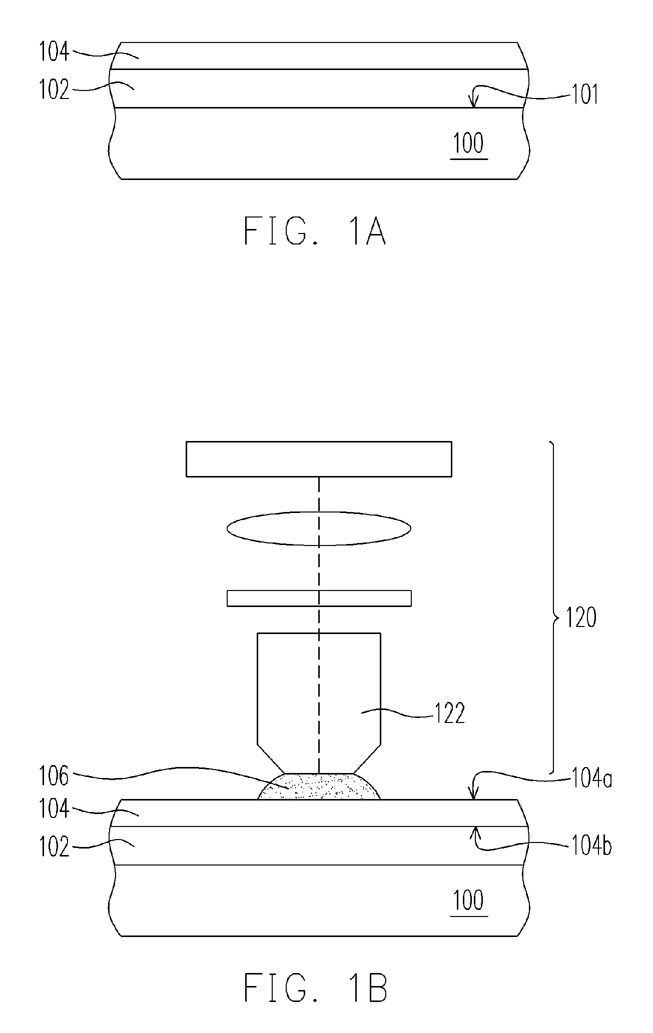
  • Description
  • Claims
  • Application Information

AI Technical Summary

Benefits of technology

[0007] It is therefore an object of the invention to provide a method for forming a material layer between the liquid and the photoresist layer in immersion lithography. The problems of micro-bubbles between the photoresist and the liquid can be alleviated, and further reaction between the photoresist and the liquid can be avoided.
[0008] To achieve these objects and advantages, and in accordance with the purpose of the invention, as embodied and broadly described herein, the invention is directed towards a method for forming a material layer between the liquid and the photoresist layer in immersion lithography. After forming a photoresist layer over the wafer, a material layer is formed on the photoresist layer and covering the photoresist layer. The material layer can be formed by spin-coating, for example. The material layer can provide a first surface wettable to the liquid (or water), and a second surface opposite to the first surface for good adhesion toward the photoresist layer. Afterwards, a liquid is provided between the material layer and a lens element of the immersion lithography system and covering the material layer.
[0009] Through forming the material layer as an interface layer between the liquid and the photoresist layer, the material layer provides good wetting toward the liquid, as well as excellent adhesion toward the photoresist layer. In addition, the material layer can act as a barrier layer, so that the molecules or particulates in the photoresist layer will not diffuse out into the liquid. Hence, the problems of bubbles or inter-reaction between the liquid and the photoresist layer can be solved and the pattern fidelity can be improved due to less defects.
[0010] Furthermore, the material layer of this invention can function as a top anti-reflection coating (ARC) layer for improving resolution of the lithography process. In this case, the material layer can be removed at the same time as the photoresist layer is developed.

Problems solved by technology

However, for the immersion lithography technology, certain technical problems still exist, such as bubbles in the immersion water or the reaction of the photoresist or the lens material to water.
Similarly, during the immersion lithography process, since the liquid is placed between the lens and the wafer and in contact with the photoresist layer over the wafer, further reaction may occur between the liquid and the photoresist layer and cause defects for lithography.

Method used


Image

  • Method for forming material layer between liquid and photoresist layer
  • Method for forming material layer between liquid and photoresist layer
  • Method for forming material layer between liquid and photoresist layer

Examples


Embodiment Construction

[0015]FIGS. 1A-1B are cross-sectional views of the process steps for forming a material layer according to one preferred embodiment of this invention.

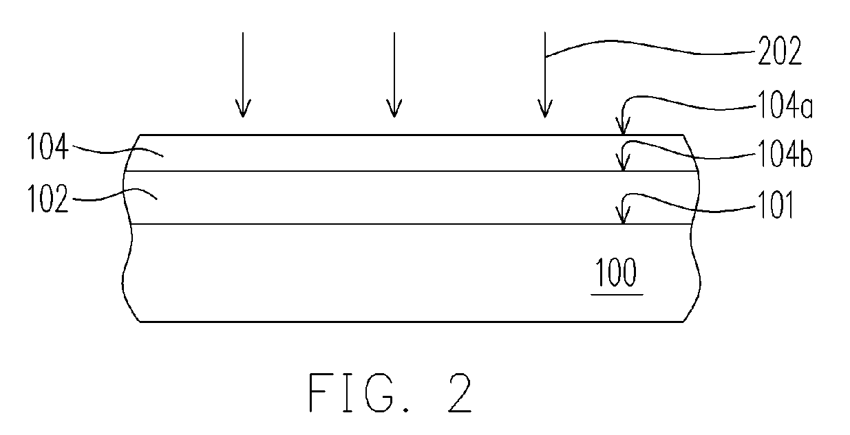
[0016] Referring to FIG. 1A, a semiconductor substrate or a semiconductor wafer 100 having a plurality of different material layers (not shown) thereon is provided. A photoresist layer 102 is formed over the active surface 101 of the wafer 100 by, for example, spin-coating. The photoresist layer 102 can be a positive photoresist layer or a negative photoresist layer. Afterwards, a material layer 104 is formed on the photoresist layer 102 and covering the photoresist layer 102. The material layer 104 can be formed by spin-coating or deposition, for example. Preferably, if the photoresist layer 102 is a 193 nm photoresist layer, the material layer 104 can be a 248 nm photoresist layer, for example. Alternatively, the material layer 104 may be comprised of a top anti-reflection coating (ARC) layer and the top ARC layer is made of fluid o...


PUM

PropertyMeasurementUnit
adhesionaaaaaaaaaa
timeaaaaaaaaaa
wettabilityaaaaaaaaaa

Abstract

The invention is directed towards a method for forming a material layer between the liquid and the photoresist layer in immersion lithography. After forming a photoresist layer over the wafer, a material layer is formed between the photoresist layer and the liquid and covering the photoresist layer. The material layer, acting as an interface layer and a barrier layer, can provide a first surface wettable to the liquid (or water), and a second surface opposite to the first surface for good adhesion toward the photoresist layer.

Description

BACKGROUND OF THE INVENTION [0001] 1. Field of Invention [0002] The present invention relates to a method for immersion lithography. More particularly, the present invention relates to a method for forming a material layer between the liquid and the photoresist layer in immersion lithography. [0003] 2. Description of Related Art [0004] In the semiconductor fabrication process, as the dimension of devices on a chip becomes smaller, the resolution required for lithography needs to be higher. Therefore, an emerging technology that uses the refractive properties of fluids to improve the resolution of lithography, called immersion lithography, has been developed in semiconductor manufacturing. In immersion lithography, a liquid is interposed between an exposure tool's projection lens and the surface of the wafer. Usually, for 193 nm immersion lithography, water appears to be the best medium for this purpose. Immersion technology offers better resolution over conventional projection litho...

Claims


Application Information

Patent Timeline
Patent Type & Authority Applications(United States)
IPC IPC(8): G03F7/20
CPCG03F7/091G03F7/2041G03F7/11
Inventor CHEN, JOSEPH
Owner UNITED MICROELECTRONICS CORP
Learn More