Method of manufacturing a semiconductor device with different lattice properties

a manufacturing method and technology of semiconductor devices, applied in the direction of semiconductor devices, electrical devices, transistors, etc., can solve the problems of reducing the processing time of transistors, reducing the time needed for electrons to pass, and cmos transistor manufacturing techniques are difficult to meet the needs of cmos transistors, so as to improve the electron mobility in the channel and reduce current loss.

Active Publication Date: 2006-11-23
SAMSUNG ELECTRONICS CO LTD
View PDF12 Cites 2 Cited by
  • Summary
  • Abstract
  • Description
  • Claims
  • Application Information

AI Technical Summary

Benefits of technology

[0017] Embodiments of the present invention relate to an apparatus including a transistor channel. The channel includes an inner portion and an outer portion. The outer portion surrounds the inner portion and includes strained silicon. Because the outer portion has a relatively large surface area and improved electron mobility due to the strained silicon, a transistor can operate more effectively and efficiently. Accordingly, the transistor can make a computer operate faster while consuming less power.
[0018] Embodiments of the present invention provide a semiconductor device and a method of manufacturing the semiconductor device capable of increasing a contact surface between a gate and a channel to reduce current loss. The lattice property of a semiconductor layer in the channel is changed to improve electron mobility. Accordingly, a semiconductor device and a method of manufacturing the semiconductor device are capable of increasing a surface contacting a gate, improving a lattice property of a semiconductor layer, improving current flow through a channel, and reducing electric power consumption of the semiconductor device.
[0021] According to embodiments of the invention, the contact surface between the channel and the gate may be increased so as to reduce current loss. Further, the lattice property of the semiconductor layer in the channel is changed to improve electron mobility in the channel.

Problems solved by technology

Further, downsizing decreases the time needed for electrons to pass through a transistor, which reduces processing time of a transistor.
Some complications exist in fabrication techniques of MOSFETs having a width less than about 0.1 μm.
There are some obstacles in manufacturing techniques of CMOS transistors, having widths less than about 0.1 μm.
These obstacles may be due to limited space charge layers, tunneling effects, and / or non-uniform doping.
These obstacles may arise during lithography, forming gate oxide layers, forming shallow source / drain extensions, and / or forming halo pocket / retrograde wells in small-scale parameters.
Reducing the semiconductor device scale has some limitations since the shape description technique for an integrated circuit has not been secured in a scale less than about 100 nm.
When the channel width is below about 90 nm, however, a short channel effect and a current leakage through the gate oxide layer may occur.
However, prior to the present invention, Tri-Gate devices have not been utilized in conjunction with strained silicon.

Method used


Image

  • Method of manufacturing a semiconductor device with different lattice properties
  • Method of manufacturing a semiconductor device with different lattice properties
  • Method of manufacturing a semiconductor device with different lattice properties

Examples


Embodiment Construction

[0028] The invention now will be described more fully hereinafter with reference to the accompanying drawings, in which exemplary embodiments of the invention are described. This invention may, however, be embodied in many different forms and should not be construed as limited to the embodiments set forth herein; rather, these embodiments are provided so that this disclosure will be thorough and complete, and will fully convey the scope of the invention to those skilled in the art. Like numbers refer to like elements throughout. The relative thickness of layers in the illustrations may be exaggerated for purposes of describing the invention.

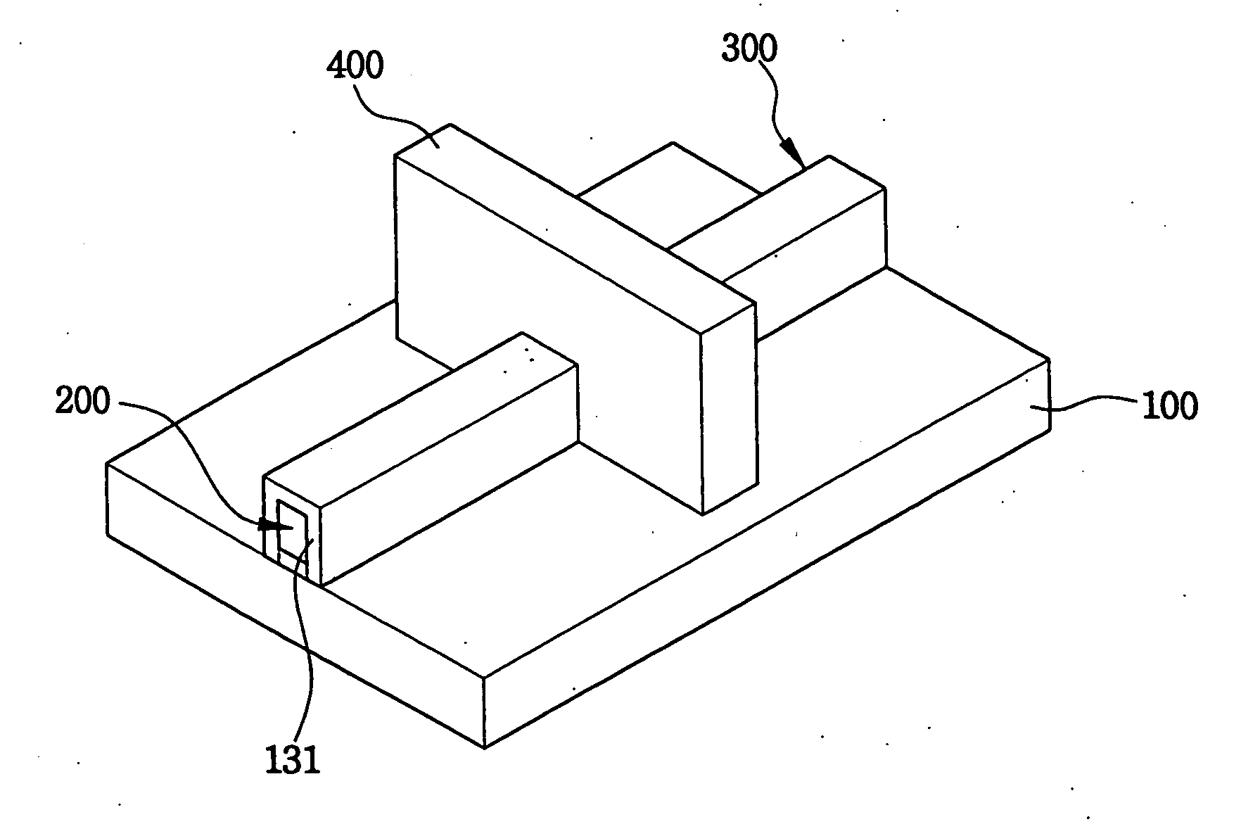
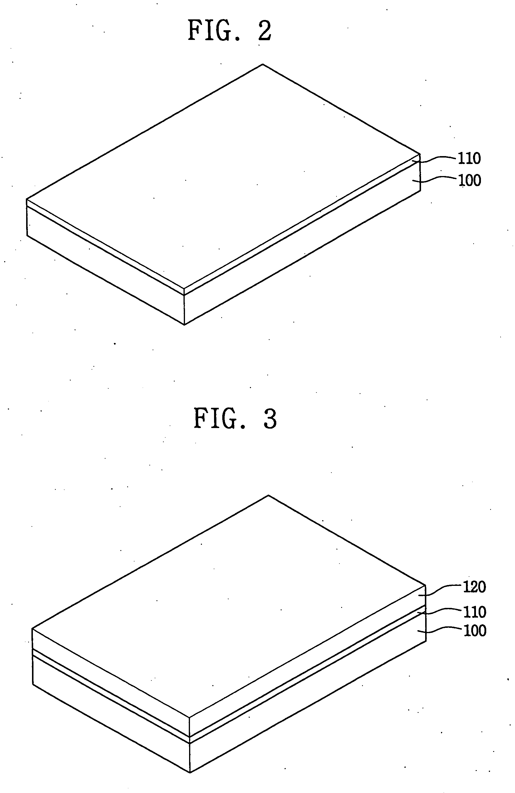
[0029] FIGS. 2 to 7 are exemplary views illustrating a method of manufacturing a semiconductor device according to embodiments of the invention. In FIG. 2, the first semiconductor layer 110 is formed on the semiconductor substrate 100. In FIG. 3, the second semiconductor layer 120 is formed on first semiconductor layer 110. The second semiconduc...


PUM


Abstract

To reduce a current loss through a channel and improve electron mobility, a first semiconductor layer and a second semiconductor layer (sequentially formed on a semiconductor substrate) have different lattice properties. The first semiconductor layer and the second semiconductor layer may be etched to form a first semiconductor pattern. A third semiconductor layer having a lattice property substantially identical to that of the first semiconductor layer may be formed over the first semiconductor pattern. The third semiconductor layer may then be etched to form a second semiconductor pattern. A gate may be formed on the second semiconductor pattern. The contact surface between the second semiconductor pattern and the gate pattern may consequently increased to reduce a current loss. Further, the lattice properties may be changed to improve electron mobility of the semiconductor layers.

Description

CROSS REFERENCE TO RELATED APPLICATION(S) [0001] This is a Divisional of, and a claim of priority is made to, U.S. non-provisional application Ser. No. 10 / 801,651, filed Mar. 17, 2004, the contents of which are incorporated herein by reference in their entirety. [0002] A claim of priority is also made to Korean Patent Application No. 2003-16450, filed on Mar. 17, 2003, the contents of which are incorporated herein by reference in their entirety.BACKGROUND OF THE INVENTION [0003] 1. Field of the Invention [0004] The present invention relates to a semiconductor device or a method of manufacturing a semiconductor device. Embodiments of the present invention are capable of reducing current loss in a semiconductor device by increasing the contact surface between channel and a gate. This reduction of current loss may be accomplished by improving electron mobility by manipulating lattice properties of the channel. [0005] 2. Description of the Related Art [0006] Transistors are semiconducto...

Claims


Application Information

Patent Timeline
Patent Type & Authority Applications(United States)
IPC IPC(8): H01L21/8234H01L21/28H01L21/3205H01L21/335H01L21/336H01L29/10H01L29/423H01L29/49H01L29/786
CPCH01L21/823828H01L29/1054Y10S257/903H01L29/785H01L29/78687H01L29/66795H01L21/18
Inventor YANG, JEONG-HWAN
Owner SAMSUNG ELECTRONICS CO LTD
Why Eureka
Try Eureka