Liquid crystal display apparatus and manufacturing method thereof

a liquid crystal display and active matrix technology, applied in electrical devices, semiconductor devices, instruments, etc., can solve the problems of defective indication, such as flicker, inability to observe the display indicated by the display light, and extreme deformation of visibility, so as to achieve high yield, suppress cell reaction, and excel in reflectance

Inactive Publication Date: 2006-11-30
MITSUBISHI ELECTRIC CORP
View PDF10 Cites 8 Cited by
  • Summary
  • Abstract
  • Description
  • Claims
  • Application Information

AI Technical Summary

Benefits of technology

[0018] According to the liquid crystal display apparatus of the invention and the manufacturing method thereof, the patterning of the second transparent conductive film is performed on the third metal film by using the same mask pattern as that used to perform the patterning of the reflective pixel electrode. Thus, the reflective pixel electrode and the second transparent conductive film having the same pattern shape as that of the reflective pixel electrode are formed. Consequently, a liquid crystal display apparatus, which can suppress the cell reaction between the reflective layer and the pixel electrode made of ITO and excels in reflectance, with high yield at low cost without increasing the number of manufacturing steps.
[0019] Also, according to the liquid crystal display apparatus of the invention and the manufacturing method thereof, the difference in work function between the reflective pixel electrode and the transparent common electrode of the counter electrode substrate can be reduced by forming the second transparent conductive film on the reflective pixel electrode. Also, the flicker and the burn-in of the liquid crystal can be reduced. Further, a liquid crystal display apparatus, which excels in quality, can be obtained at low cost with high yield.
[0020] Also, because the thickness of the second transparent conductive film is equal to or more than 5 nm, the reflecting layer made of Al or Al-alloy can be completely covered with the second transparent conductive film. Thus, the invention has advantages that in the photolithography process, the developer can be prevented from entering the boundary layer between the pixel electrode and the lower reflecting layer, and that the cell reaction can be suppressed. Further, because the thickness of the second transparent conductive film is equal to or less than 15 nm, the invention has an advantage that reduction in the reflectance can be suppressed.

Problems solved by technology

The transmissive type liquid crystal display apparatus has a problem that in a case where ambient light is very bright, a display indicated by displaying-light cannot be observed because the displaying light is dark in comparison with the displaying-light.
Also, the reflective type liquid crystal display apparatus has a problem that visibility is extremely degraded in a case where ambient light is dark.
Further, in a case where an Al-alloy is used as the material of a reflective pixel electrode in a semi-transmissive liquid crystal display apparatus, as described above, a defective indication, such as a flicker, occurs due to a difference in a work function between the material of the reflective pixel electrode and that, such as ITO, of the transparent conductive film used as that of the color filter substrate serving as the counter substrate.
However, the following problem occurs in the semi-transmissive liquid crystal display apparatus.
In a case where the coverage of the Mo-alley on a pattern edge of the pixel electrode is poor and a crack or the like is present, the simultaneous contact of the developer with both of the ITO and the Al-material may occur due to the crack in the Mo-alloy.
Therefore, this technique has problems that the corrosion-resistance of the electrode is not necessarily sufficient, and that there is the necessity for increasing the number of steps of forming films to form the Mo-alley film as the foundation thereby to increase the manufacturing cost of the display device.
Also, in a case where an Al-alloy is used as the material of the reflective pixel electrode in the semi-transmissive type liquid crystal display apparatus, a defective indication, such as a flicker, occurs due to the difference between the Al-alloy and the material of the transparent conductive film, such as ITO, used as the counter electrode on the color filter substrate serving as the counter substrate.
Thus, when etching is performed on the reflective pixel electrode, the source electrode is eroded by etchant for the reflective pixel electrode, so that disconnection of the source electrode may occur.
Accordingly, this technique has problems that a new mask pattern is needed, that the number of steps increases, and that the manufacturing cost of the display apparatus increases.
Thus, this technique has a problem that the reflectance of the reflective pixel electrode is degraded.

Method used


Image

  • Liquid crystal display apparatus and manufacturing method thereof
  • Liquid crystal display apparatus and manufacturing method thereof
  • Liquid crystal display apparatus and manufacturing method thereof

Examples


first embodiment

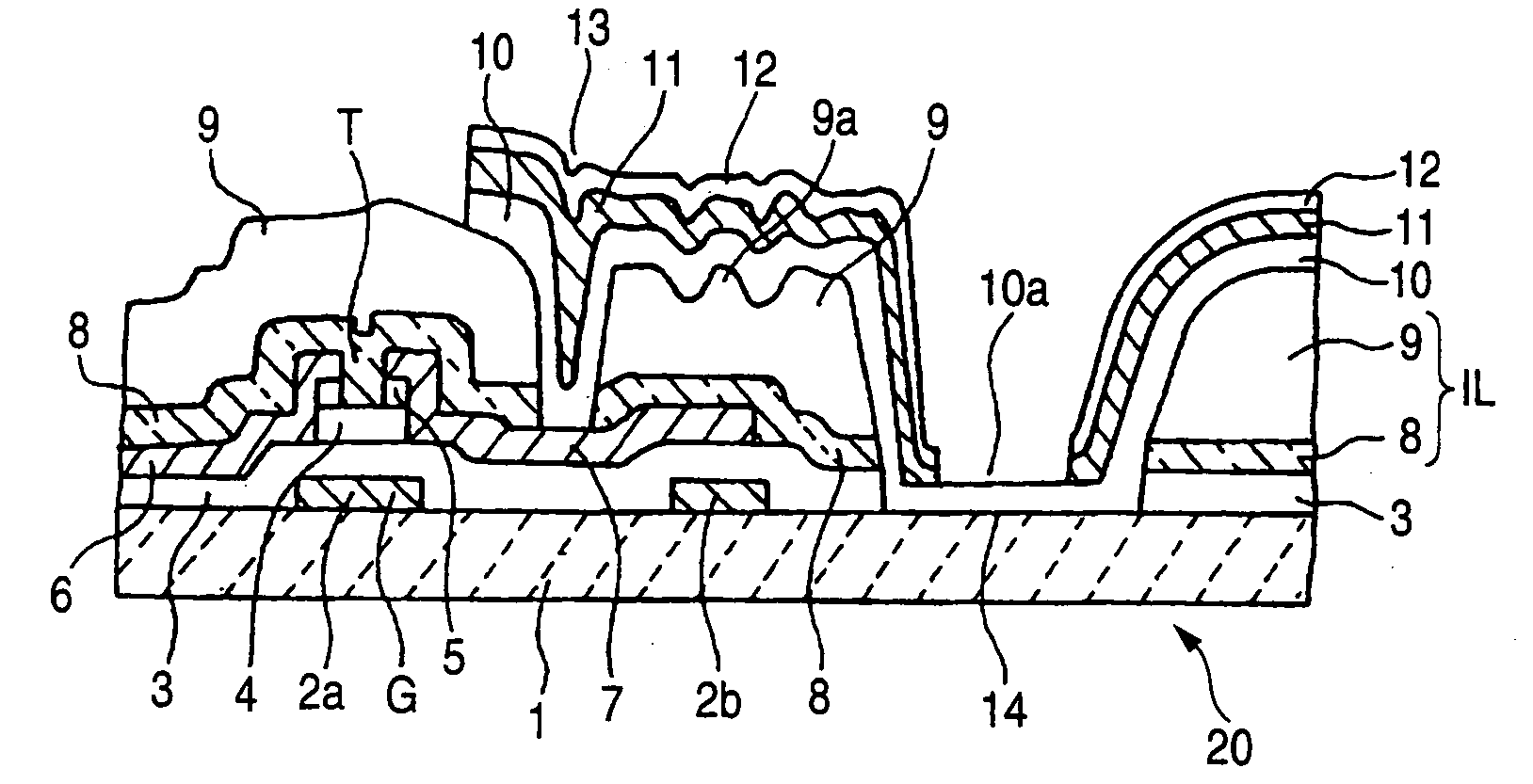
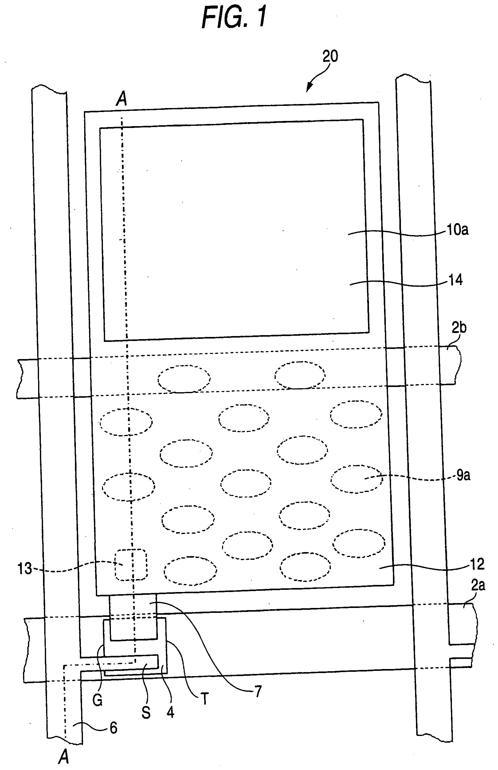
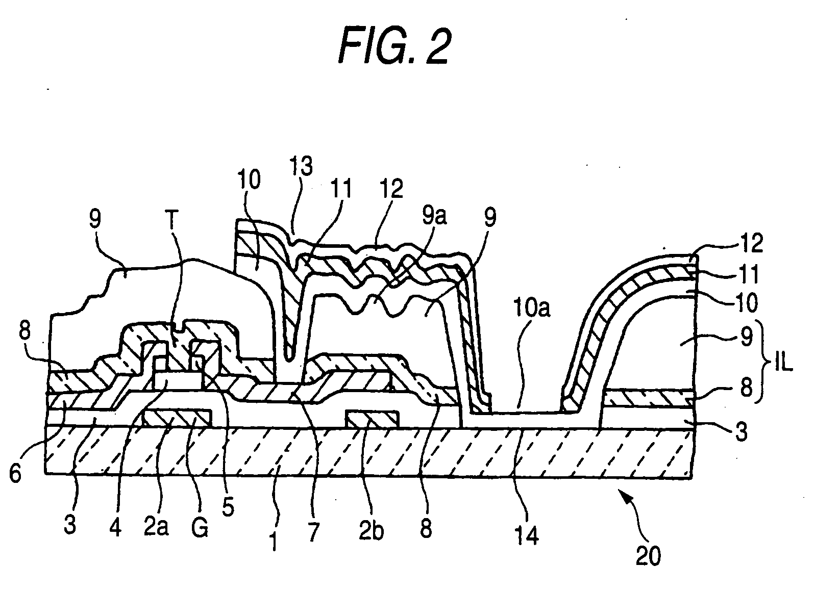
[0024] Hereinafter, a first embodiment, which is a best mode for carrying out the invention, is described. FIG. 1 is a plan view illustrating one pixel part of a semi-transmissive type liquid crystal display apparatus that is the first embodiment of the invention. FIG. 2 is a cross-sectional view taken along line A-A shown in FIG. 1 and illustrates the configuration of a cross-section of a part of the semi-transmissive type liquid crystal display apparatus shown in FIG. 1. In these figures, like or corresponding portions are designated by like reference numerals. As shown in FIGS. 1 and 2, the semi-transmissive type liquid crystal display apparatus is configured so that each pixel part provided on a TFT array substrate 20 has a transparent pixel electrode 10a adapted to transmit light, and a reflective pixel electrode 11 adapted to reflect light. A counter electrode substrate (not shown) having a transparent common electrode is disposed to be opposed to this TFT array substrate 20. ...


PUM


Abstract

A liquid crystal apparatus includes a TFT array substrate which includes gate wirings having a gate electrode, source wirings having a source electrode, a thin film transistor having the gate electrode, a semiconductor layer, the source electrode, and a drain electrode, an interlayer insulating film provided above the thin film transistor and the gate and source wirings, a transparent pixel electrode having a first transparent conductive film connected to the drain electrode through a contact hole, and put into contact with a surface of a insulating substrate through a pixel opening provided in a gate insulating film and the interlayer insulating film, a reflective pixel electrode made of an Al-alloy connected to the drain electrode, and a second transparent conductive film formed on the reflective electrode. The second transparent conductive film has a same pattern shape as the reflective pixel electrode and a thickness thereof is at least 5 nm.

Description

BACKGROUND OF THE INVENTION [0001] 1. Field of the Invention [0002] The present invention relates to an active matrix type liquid crystal display apparatus (TFT-LCD) using a thin film transistor (TFT) as a switching element and to a manufacturing method therefor and, more particularly, to a method of manufacturing a TFT array substrate, which has a transparent conductive film provided on a reflective pixel electrode, at low cost. [0003] 2. Description of the Related Art [0004] The active matrix type liquid crystal display apparatus is configured so that a liquid crystal material is placed between a TFT array substrate, in which thin film transistors are arranged in a matrix manner on a glass substrate, and a color filter substrate having counter electrodes, and that the orientation of the liquid crystal material is controlled by the electrodes formed on the substrates to thereby display an image. The active matrix type liquid crystal display apparatuses have widely been developed as...

Claims


Application Information

Patent Timeline
Patent Type & Authority Applications(United States)
IPC IPC(8): H01L29/82
CPCG02F1/133371G02F1/136227G02F1/133555G02F1/136
Inventor NAKAHORI, TADAKIISHIGA, NOBUAKINAGAYAMA, KENSUKEYOSHIDA, TAKUJI
Owner MITSUBISHI ELECTRIC CORP
Why Eureka
Try Eureka