Imaging device

a technology of imaging device and discharge tube, which is applied in the field of imaging, can solve the problems of insufficient low-resolution conventional imaging device, and achieve the effects of improving color reproduction quality, higher luminance light, and different color

Inactive Publication Date: 2006-11-30
PANASONIC LIQUID CRYSTAL DISPLAY CO LTD +1
View PDF1 Cites 4 Cited by
  • Summary
  • Abstract
  • Description
  • Claims
  • Application Information

AI Technical Summary

Benefits of technology

[0045] The phosphor layers for use in the present invention may further contain or may be present in combination with one or more other phosphors with different compositions as a phosphor mixture. Particularly, they preferably further contain at least one phosphor such as Y3(Al, Ga)5O12:Tb phosphor, Zn2SiO4:Mn phosphor, LaOCl:Tb phosphor, InBO3:Tb phosphor, LaPO4:Tb, Ce phosphor, Y2O3:Eu phosphor, BaMgAl10O17:Eu phosphor, and ZnS phosphor. The resulting phosphor mixture can emit higher luminance light, provide better color reproduction quality, have a different color, or have a longer lifetime.
[0046] The conventional phosphor layers must have a thickness exceeding 40 μm, for high luminance. In contrast, the phosphor layers according to the present invention can provide satisfactorily high luminance that is practically applicable, even if they have a thickness of 40 μm or less, by using the phosphors relating to the present invention. The present invention can provide imaging devices showing high resolution and high luminance by using the phosphors in a phosphor layer having a thickness of 40 μm or less.
[0047] The resulting imaging devices including phosphor layers containing the phosphor according to the present invention can produce good-quality images in practical use.
[0048] This will be explained, using a projection display as an example. The projection display includes three projection tubes that are for discrete red (R), blue (B), and green (G) colors. Phosphors that are deposited to the face plate of the green emitting projection tube preferably contain any of the phosphors relating to the present invention alone or as a green emitting phosphor mixture in combination with one or more other phosphors. This can yield an imaging device featuring a longer lifetime.
[0049] The phosphors relating to the prevent invention are also used in cathode-ray tubes for direct-viewing display (hereinafter referred to as direct-viewing tubes). Green emitting phosphors of the phosphors of three primary colors to be applied to a face plate are preferably any of the phosphors relating to the present invention alone or as a green-emitting phosphor mixture in combination with one or more other phosphors. This can yield an imaging device featuring fine green emission color, a longer lifetime, shorter afterglow, and good image quality.
[0050] It is also advisable to apply a phosphor layer comprising the phosphors relating to the present invention to an imaging device using low energy electron beams, such as a field-emitter display (abbreviated to FED). This can yield an imaging device featuring a longer lifetime.

Problems solved by technology

These conventional imaging devices are insufficient in low resolution.

Method used


Image

  • Imaging device
  • Imaging device
  • Imaging device

Examples


embodiment 2

[0105] The luminance was measured at a distance of several tens of centimeters using a luminance meter. The spot diameter was also measured by the procedure in

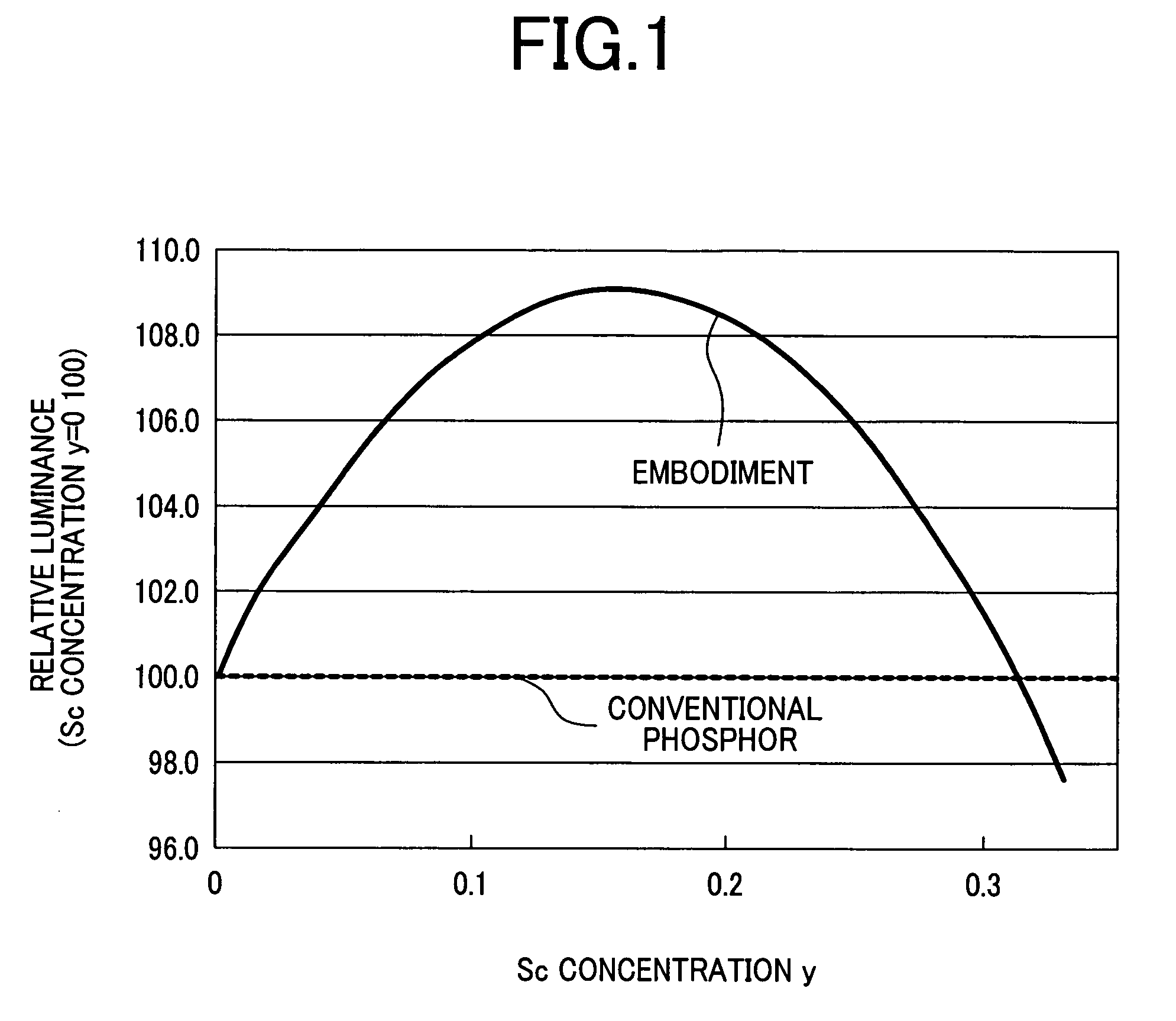
[0106] These results show that the cathode-ray tubes prepared according to the present invention show higher resolution than conventional equivalents and show luminance properties equal to or higher than the conventional equivalents. Specifically, the present invention provides imaging devices showing high resolution and high luminance and producing high-quality images.

[0107] A projection television imaging device having a layer of the phosphors according to the present invention as a green emitting layer for image display was prepared.

embodiment 3

[0108] Initially, a 18-cm projection tube for green images according to the present invention was prepared by the procedure of The projection television imaging device was then prepared using the 18-cm projection tube for green images in combination with a projection tube for red images and a projection tube for blue images.

[0109]FIG. 9 is a schematic diagram of the projection television imaging device according to the present invention. FIG. 9 illustrates a cathode-ray tube for red images 5, a cathode-ray tube 6 for green images according to the present invention, a cathode-ray tube 7 for blue images, and a screen 8 arranged at predetermined distances so as to face these tubes. Lenses 9 are located between the screen and the projection tubes, aligned with the axis of each tube. A monochromatic image reproduced on the face plate of each projection tube is converged and enlarged through lenses and projected on the screen 8. Three colors reproduced by the tubes are combined into a co...

embodiment 4

[0111] Measurements were made for the light emission properties of the projection television imaging device of Embodiment 4 in methods as will be described below. Luminance was measured by a luminance meter from the point at a distance of several tens of centimeters. Assuming the luminance of the current standard product of the same device in conventional use to be 100, the luminance measurements were represented in relative luminance. All measurements were made under the conditions that the phosphor layer in area of 102 mm long and 76 mm wide is excited by being irradiated with 0.1- to 10-mA cathode rays at a voltage of 30 kV.

[0112] The phosphor emission color was measured by a chromaticity meter from the point at a distance of several tens of centimeters. Emission color comparison was made in terms of “y” values of chromaticity on the x-y chromaticity coordinates.

[0113] The device properties with regard to luminance degradation were evaluated by a test in which the phosphor layer...


PUM

PropertyMeasurementUnit
thicknessaaaaaaaaaa
thicknessaaaaaaaaaa
thicknessaaaaaaaaaa

Abstract

To provide an imaging device that shows high resolution and high luminance and produces good-quality images, an imaging device includes phosphor layer having a thickness of 40 μm or less and containing a phosphor having a composition represented by chemical formula: Y2−x−yTbxScySiO5, wherein “x” and “y” are atomic ratios and satisfy the following conditions: 0<x≦1 and 0<y≦1. The phosphor preferably has a strongest diffraction peak at diffraction angle 2θ of 30.65° to 30.9° in X-ray diffraction for better properties. The phosphor can be prepared by firing a mixture of a compound containing Y, Sc, and Tb with a compound containing Si.

Description

CLAIM OF PRIORITY [0001] The present application claims priority from Japanese application JP 2005-158357 filed on May 31, 2005, the content of which is hereby incorporated by reference into this application. BACKGROUND OF THE INVENTION [0002] 1. Field of the Invention [0003] The present invention relates to imaging. More specifically, it relates to imaging devices that have phosphor layers showing high resolution and high luminance and being typically suitable for projection cathode-ray tubes. [0004] 2. Description of the Related Art [0005] Imaging devices discussed herein are those for imaging based on image data through light emission in such a way that phosphors are excited by irradiation of electron beams or ultraviolet rays. Examples thereof are cathode-ray tubes (especially, projection cathode-ray tubes), display panels using low energy electron beams, such as field-emitter displays (FEDs), and plasma display panels (PDPs). The field-emitter displays herein are displays havin...

Claims


Application Information

Patent Timeline
Patent Type & Authority Applications(United States)
IPC IPC(8): H01J63/04H01J1/62C09K11/08C09K11/56C09K11/78C09K11/79H01J11/22H01J11/24H01J11/34H01J11/42H01J29/20H01J31/10H01J31/12H01J61/44
CPCC09K11/7774H01J1/63H01J2329/20H01J2211/42H01J61/42C09K11/77742
Inventor IMAMURA, SHINKOMATSU, MASAAKIMATSUKIYO, HIDETSUGUSHIIKI, MASATOSHI
Owner PANASONIC LIQUID CRYSTAL DISPLAY CO LTD
Why Eureka
Try Eureka