Semiconductor device

a technology of semiconductors and capacitors, applied in the direction of burglar alarm mechanical actuation, burglar alarm by hand-portable objects removal, instruments, etc., to achieve the effect of reducing the occupation area of capacitors and easy adjustmen

Inactive Publication Date: 2006-11-30
SEMICON ENERGY LAB CO LTD
View PDF5 Cites 19 Cited by
  • Summary
  • Abstract
  • Description
  • Claims
  • Application Information

AI Technical Summary

Benefits of technology

[0020] By implementing the present invention, a semiconductor device in which resonance frequency can be easily adjusted to be the desired frequency can be obtaine

Problems solved by technology

However, when capacitance of the semiconductor device is formed with the use of the plate-shaped conductors, an arrangement area becomes wide; therefore, a defect is caused in the case of examining miniaturization of the semiconductor device.
Further, when capacitance of the semiconductor device is formed by only an equivalent capacitance value, a trouble is caused in a case where capacitance is adjusted by a value

Method used


Image

  • Semiconductor device
  • Semiconductor device
  • Semiconductor device

Examples


embodiment mode 1

[0035] One mode of the present invention will be described with reference to FIGS. 1A and 1B, FIGS. 2A and 2B, and FIGS. 3A and 3B.

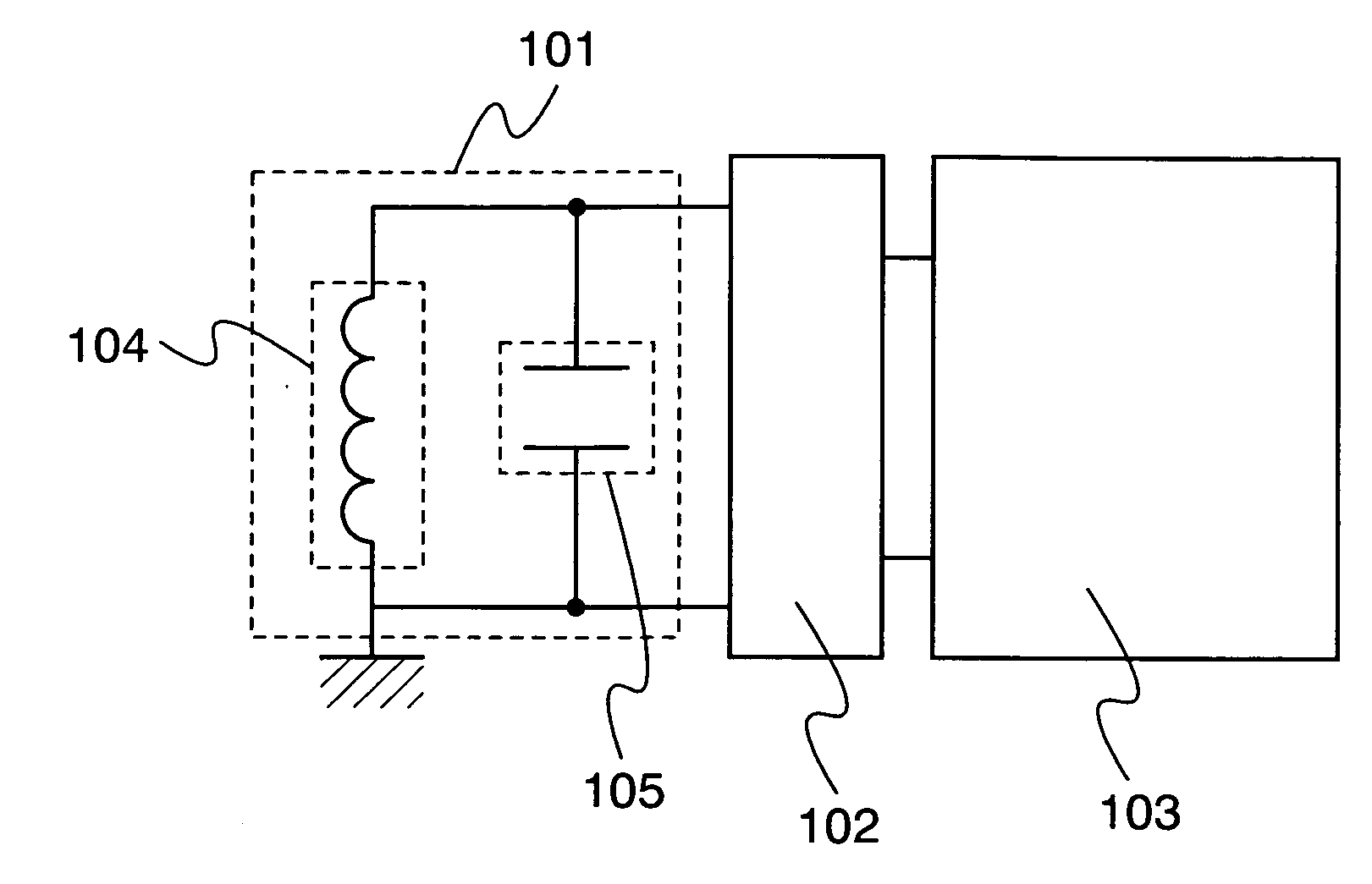
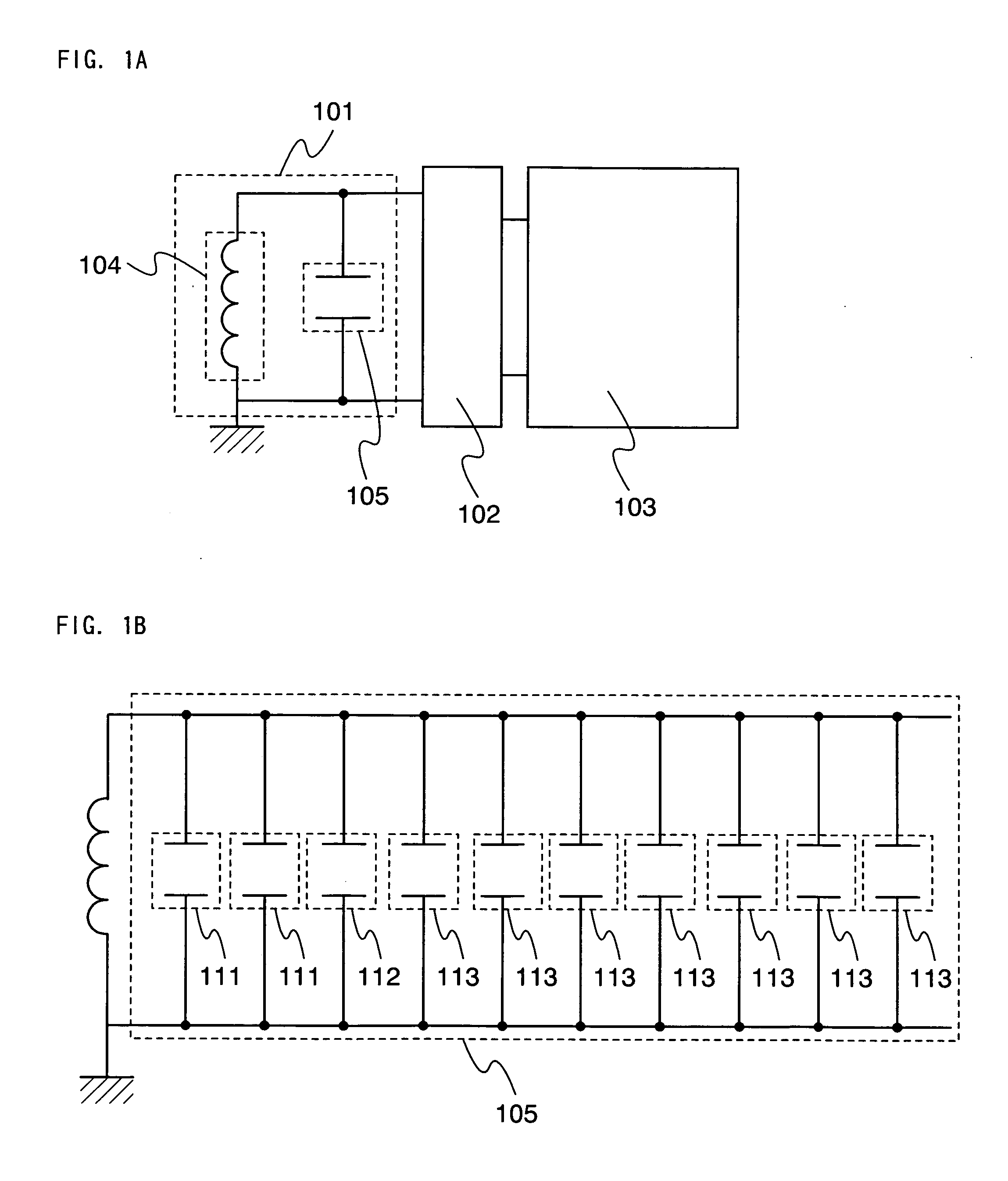
[0036] As shown in FIG. 1A, a semiconductor device of the present invention includes a resonance circuit 101, a modulation / demodulation circuit 102 for modulating an electromagnetic wave, and an arithmetic circuit 103 for processing a signal. The resonance circuit 101 includes an antenna 104 and a capacitor 105.

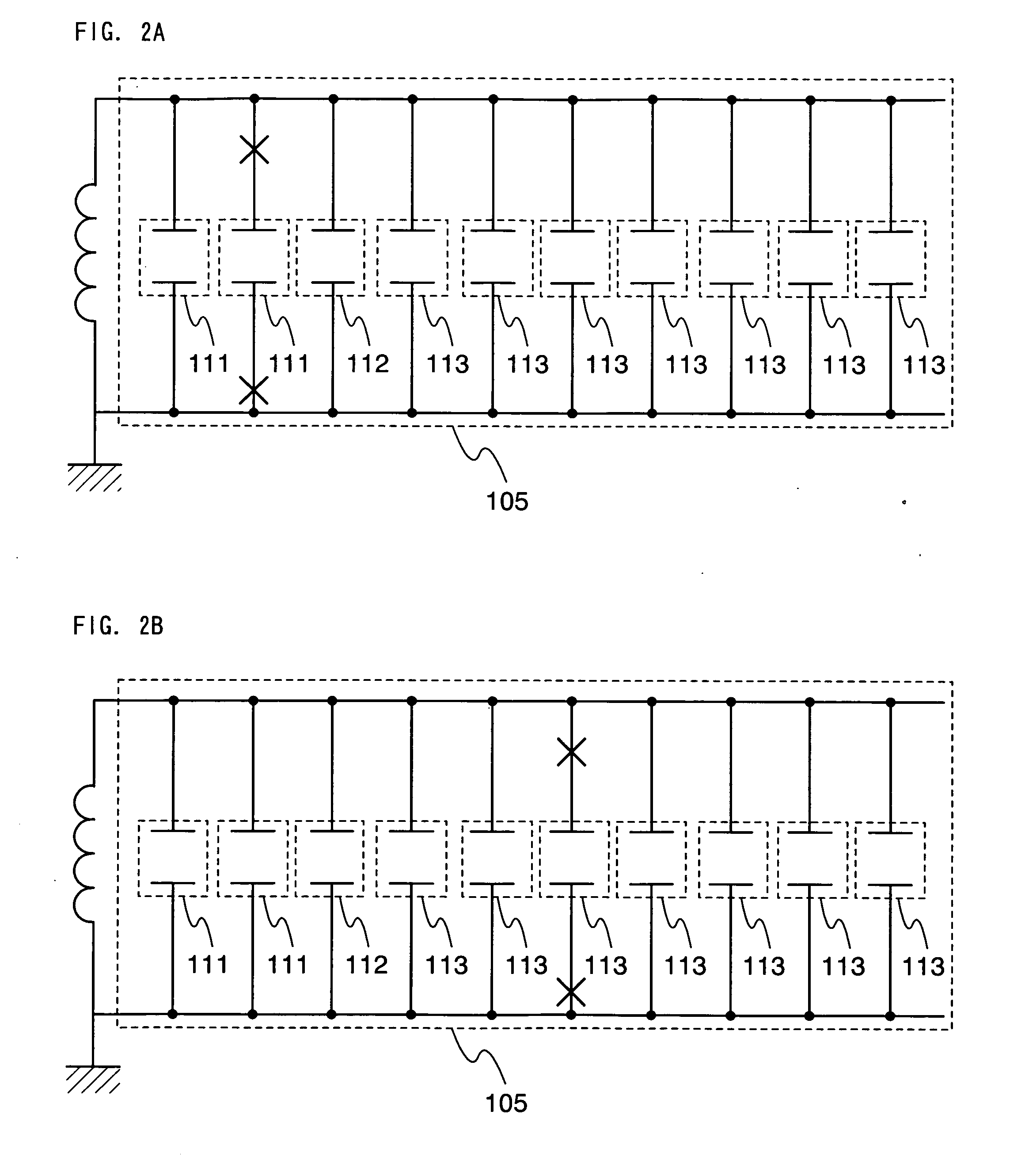
[0037] A configuration of the capacitor 105 is described with the use of FIG. 1B. In the semiconductor device of the present embodiment mode, the capacitor 105 is formed of two pieces of first capacitor 111, a piece of second capacitor 112, and seven pieces of third capacitor 113, and these capacitors are connected in parallel. The first capacitor 111, the second capacitor 112, and the third capacitors 113 have different capacitance values from each other. When a capacitance value of the first capacitor 111 is C1, a capacitance value of the seco...

embodiment mode 2

[0043] In the present embodiment mode, one mode of a method for manufacturing a semiconductor device of the present invention will be described with the use of FIGS. 5A to 5C, FIGS. 6A and 6B, FIGS. 7A and 7B, and FIG. 8.

[0044] Here, a cross sectional structure of a transistor provided in a modulation circuit and a cross sectional structure of a capacitor provided in a resonance circuit are specifically described. Accordingly, cross sectional views of a modulation circuit portion 761 and a resonance circuit portion 762 are shown in FIGS. 5A to 5C, FIGS. 6A and 6B, FIGS. 7A and 7B, and FIG. 8.

[0045] A peeling layer 702 is formed on one surface of a substrate 701 (see FIG. 5A). The substrate 701 has an insulating surface. In a case where the substrate is made of glass, an area and a shape thereof is not particularly limited. Therefore, when a substrate having a rectangular shape of which one side is one meter or more, for example, is used as the substrate 701, productivity can be re...

embodiment mode 3

[0077] A structure of a transistor and a capacitor provided in a semiconductor device of the present invention is not limited to the structure described in Embodiment Mode 2. In the present embodiment mode, a mode of a transistor capacitor having different structure from that described in Embodiment Mode 2 will be described with reference to FIGS. 13A and 13B.

[0078] It is to be noted that former steps of forming a gate insulating layer and subsequent steps of forming an insulating layer to cover a transistor and the like are the same as the steps in Embodiment Mode 2; therefore, the description in Embodiment Mode 2 is applied to the steps.

[0079] A first conductive layer and a second conductive layer are stacked over a gate insulating layer 908. It is to be noted that the first and second conductive layers are similar to the first and second conductive layers in Embodiment Mode 2. A mask formed of a resist is formed by photolithography over the second conductive layer that is provi...


PUM


Abstract

It is an object of the present invention to provide a semiconductor device in which an arrangement area of capacitance can be reduced and resonance frequency can be easily adjusted. The semiconductor device includes an antenna and a resonance circuit including a capacitor connected to the antenna in parallel where the capacitor is formed by connecting x pieces of first capacitor (x is an arbitrary natural number), y pieces of second capacitor (y is an arbitrary natural number), and z pieces of third capacitor (z is an arbitrary natural number) in parallel; and the first capacitor, the second capacitor, and the third capacitor have different capacitance values from each other. It is preferable that each of the first capacitor, the second capacitor, and the third capacitor be a MIS capacitor. Further, at least one of the first capacitor, the second capacitor, and the third capacitor is preferably formed by connecting a plurality of capacitors in parallel.

Description

BACKGROUND OF THE INVENTION [0001] 1. Field of the Invention [0002] The present invention relates to a semiconductor device having a resonance circuit. The present invention also relates to a semiconductor device capable of transmitting and receiving data by wireless communication. [0003] 2. Description of the Related Art [0004] In recent years, an environment where information network can be accessed at any time in any situations, which is referred to as a ubiquitous information society, has been facilitated. In such an environment, individual recognition technology has attracted attention. For example, there is technology that can be used for production, management, and the like, in which a history of an object is clarified by giving an ID (an individual recognition code) to an individual object. Above all, a semiconductor device capable of transmitting and receiving data by wireless communication is beginning to be utilized [0005] In a semiconductor device of a transmitter / receiv...

Claims


Application Information

Patent Timeline
IPC IPC(8): G08B13/14
CPCG06K19/07749G06K19/0723H01L21/485
Inventor SHIONOIRI, YUTAKAATSUMI, TOMOAKIINOUE, HIROKI
Owner SEMICON ENERGY LAB CO LTD
Why Eureka
Try Eureka