Power semiconductor module

Inactive Publication Date: 2006-12-21
FUJI ELECTRIC CO LTD
View PDF16 Cites 17 Cited by
  • Summary
  • Abstract
  • Description
  • Claims
  • Application Information

AI Technical Summary

Benefits of technology

[0030] A frame-shaped magnetic core, set around a module package according to the invention, facilitates suppressing the noise current without enlarging the module package and facilitates reducing the power semiconductor module size.
[0031] The magnetic core set around the module package facilitates the replacement thereof to another magnetic core that exhibits an optimum inductance value at the noise frequency that depends on the peripheral circuit condi

Problems solved by technology

In the above described conventional electric power converter including power semiconductor modules 2, excessively large switching noises are caused by the switching of the IGBTs and such power semiconductor devices.
The excessively large switching noises further cause malfunctions of the other apparatus and equipments disposed around the electric power converter, noises in the other apparatus and equipments and such hazards.
However, it is impossible for the conventional technique 1 to replace the filter element, even if it is necessary.
Since the conventional technique 1 houses the filter element in a package, the package is inevitably large.
These problems are also posed on the conventional technique described in FIG. 14.
Since large wiring parts such as wide area copper bars are connected to the power module terminal usually to make a high current flow, it is impossible to set the noise red

Method used


Image

  • Power semiconductor module
  • Power semiconductor module
  • Power semiconductor module

Examples


first embodiment

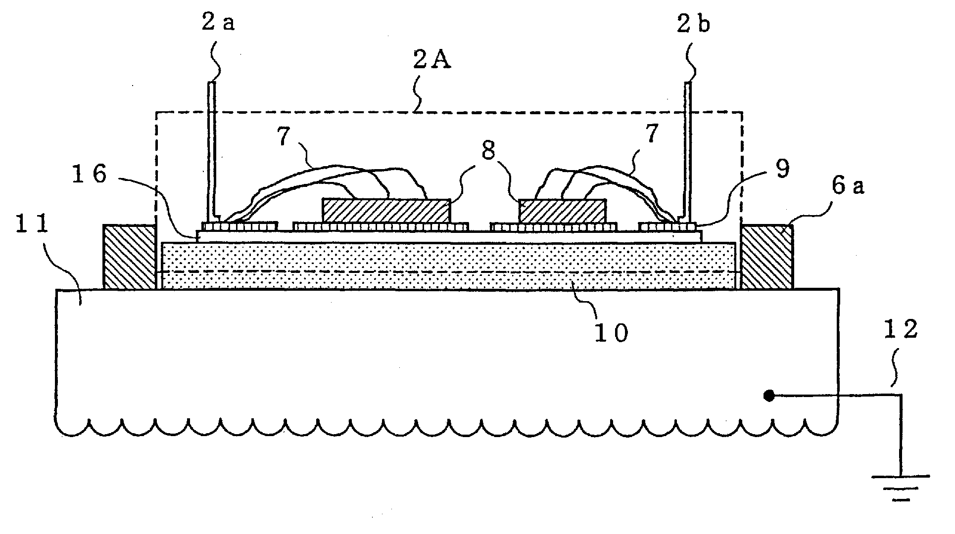
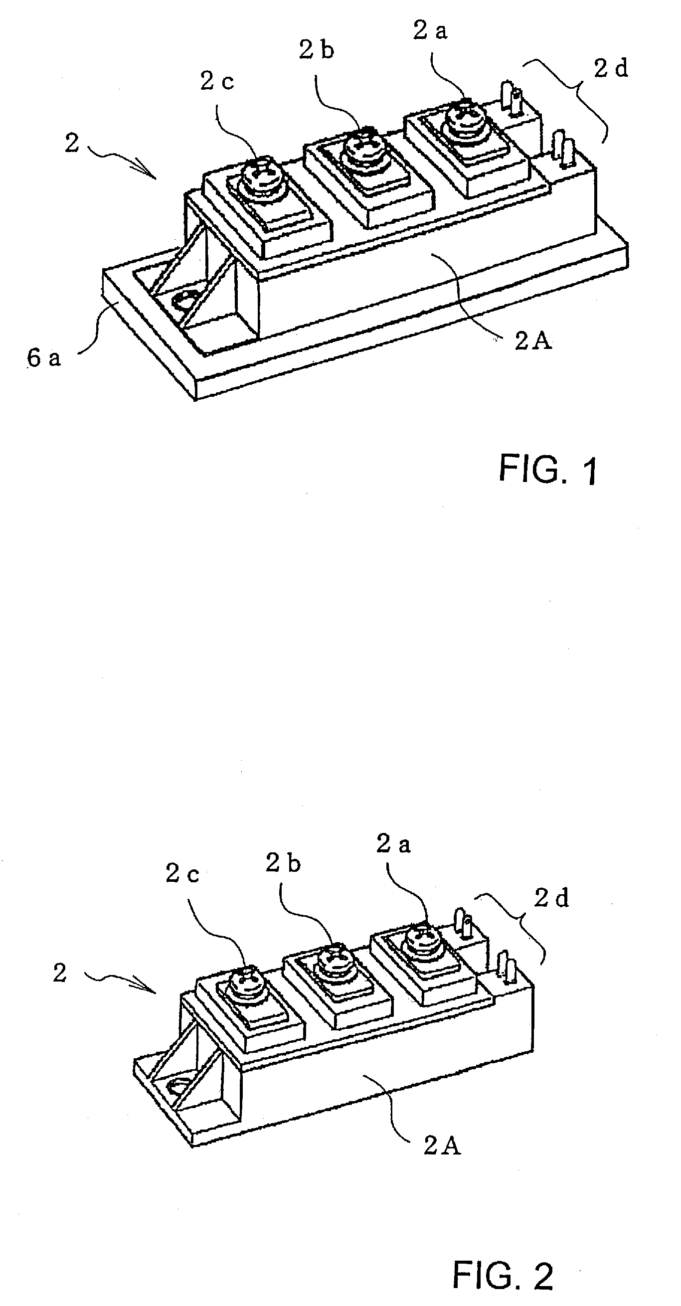
[0049]FIG. 1 is a perspective view of a power semiconductor module according to the invention including a module package 2A and a magnetic core 6a set around module package 2A. FIG. 2 is a perspective view of module package 2A shown in FIG. 1.

[0050] Referring now to these figures, power semiconductor module 2 has a structure same with that of the conventional power semiconductor module. The entire semiconductor module 2 is shaped almost with a rectangular parallelepiped. Semiconductor module 2 includes a module package 2A made of a resin and such an insulator. Module package 2A houses IGBTs as power semiconductor devices for the upper and lower arms for a phase and free wheel diodes therein as shown in FIG. 13. On the upper surface of module package 2A, DC input terminals 2a and 2b and an AC output terminal 2c are arranged appropriately. Control terminals 2d for connecting the IGBTs to the driver circuit outside module package 2A are disposed on the upper surface of module package 2...

sixth embodiment

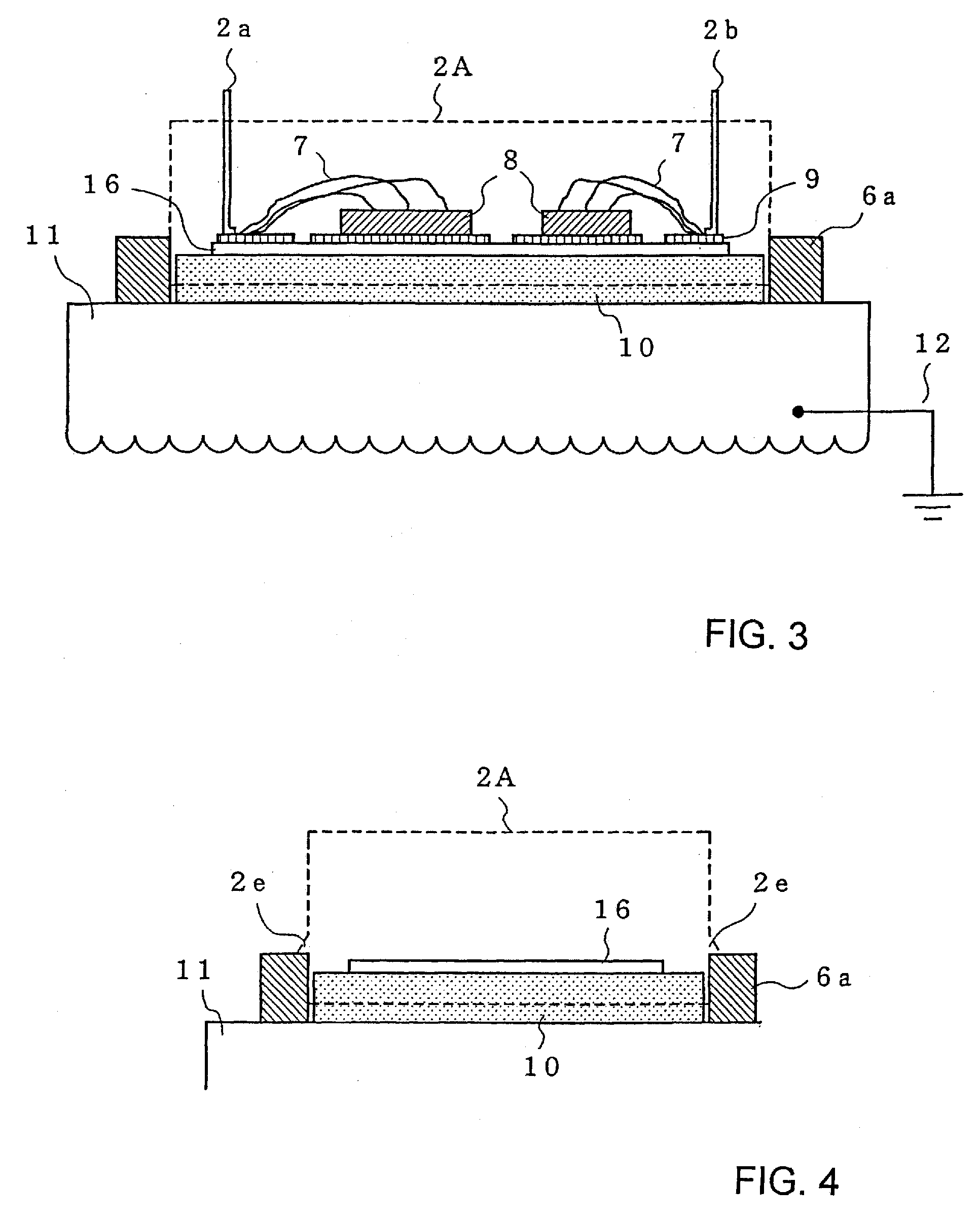
[0065] Although the magnetic core inductance is given by the numerical formula (1) as described earlier, the relative permeability μr of the magnetic core exhibits frequency dependence. Since μr is smaller as the frequency is higher, the inductance value becomes smaller as the frequency increases, making it harder to suppress the noises. magnetic core 6a made of a material that exhibits the predetermined permeability at a low frequency and magnetic core 6g made of a material that exhibits the other predetermined permeability at a high frequency are combined and laminated. The laminate of magnetic cores 6a and 6g is set around the lower portion of module package 2A to obtain certain inductance values over a wide frequency range between a low frequency and a high frequency and to obtain noise reduction effects over the wide frequency range. In FIG. 12, the inside of module package 2A is shown only partly.

[0066] In the power semiconductor devices according to the first through sixth e...


PUM


Abstract

The power semiconductor module includes a module package housing power semiconductor devices therein and a magnetic core set around the module package, such that magnetic core surrounds the power semiconductor devices such as IGBTs. Alternatively, the magnetic core is built in the module package such that the outer circumference faces of magnetic core and the side faces of module package form side faces of the power semiconductor module. The power semiconductor module according to the invention facilitates replacing the magnetic core, setting the magnetic core around the module package thereof, reducing the size thereof, simplifying the structure thereof, and easy manufacture thereof.

Description

FIELD OF THE INVENTION [0001] The present invention relates to a power semiconductor module that switches on and off power semiconductor devices incorporated therein to convert electric power. Specifically, the present invention relates to techniques for reducing the switching losses caused by the switching of the power semiconductor devices. BACKGROUND OF THE INVENTION [0002]FIG. 13 is a block circuit diagram of a conventional electric power converter including power semiconductor modules. In FIG. 13, a DC power supply 1, power semiconductor modules 2U, 2V and 2W, a motor 3 as a load, and a driver circuit 4 for driving power semiconductor modules 2U, 2V and 2W for the respective phases are shown. Each power semiconductor module 2U, 2V or 2W includes two insulated gate bipolar transistors (hereinafter referred to as “IGBTs”) connected in series and two free wheel diodes connected in opposite parallel to the respective IGBTs. Power semiconductor modules 2U, 2V and 2W for the respecti...

Claims


Application Information

Patent Timeline
IPC IPC(8): H01L31/111
CPCH01L24/45H01L24/49H01L2924/1305H01L2924/12041H01L2224/49111H01L2924/014H01L2924/01068H01L2924/01006H02M7/003H01L2924/3025H01L2924/3011H01L25/072H01L25/165H01L2224/45124H01L2224/48091H01L2224/48227H01L2924/01004H01L2924/01005H01L2924/01013H01L2924/01015H01L2924/01029H01L2924/01033H01L2924/01078H01L2924/01082H01L2924/01083H01L2924/13055H01L2924/14H01L2924/30107H01L2924/00014H01L2924/00H01L2924/181H01L24/48H01L2924/00012
Inventor TAKUBO, HIROMU
Owner FUJI ELECTRIC CO LTD
Why Eureka
Try Eureka