Optical modulator

a technology of optical modulator and optical axis, applied in the field of optical modulator, can solve the problems of failure due to the magnification of the spectral width, low power consumption and inability to realize the downsizing of the system, and achieve the effect of reducing the number of elements, excellent cost performance, and minimizing the optical modulator itsel

Active Publication Date: 2006-12-21
SUMITOMO OSAKA CEMENT CO LTD
View PDF11 Cites 9 Cited by
  • Summary
  • Abstract
  • Description
  • Claims
  • Application Information

AI Technical Summary

Benefits of technology

[0044] By the invention of claim 5, since the light branch means, the SSB modulation means, the intensity adjustment means, the phase adjustment means, and the multiplexing means are mounted on the same substrate having the electrooptic effect, it is possible to miniaturize the optical modulator itself and to reduce the number of elements such as peripheral circuits. Thus, it is possible to provide an optical modulator having excellent cost performance.
[0045] By the invention of claim 6, since the phase modulation means is provided at the previous stage of the light branch means or between the light branch means and the SSB modulation means, it is possible to spread out the light source carrier to a plurality of light source carrier components and to magnify a spectra

Problems solved by technology

According to the method shown in FIG. 1, SBS resistance increases and high-output light can be input to the transmission fiber, but a failure due to the magnification of the spectral width occurs.
Furthermore,

Method used


Image

  • Optical modulator
  • Optical modulator
  • Optical modulator

Examples


Embodiment Construction

[0096] Hereinafter, exemplary embodiments of the present invention will be described in detail.

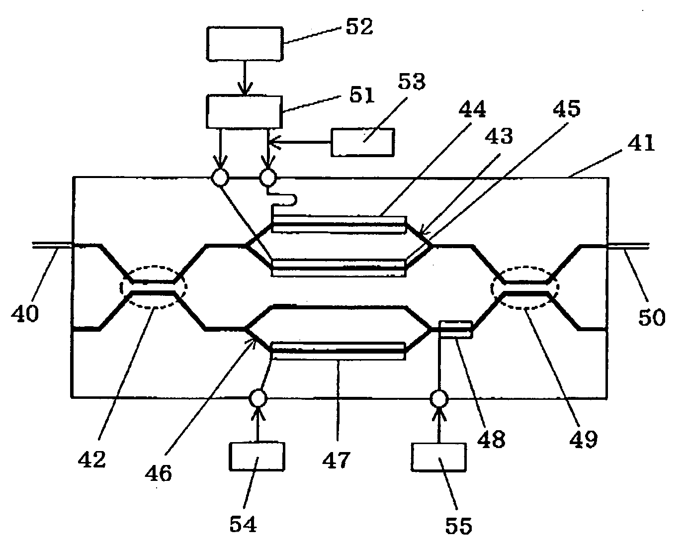
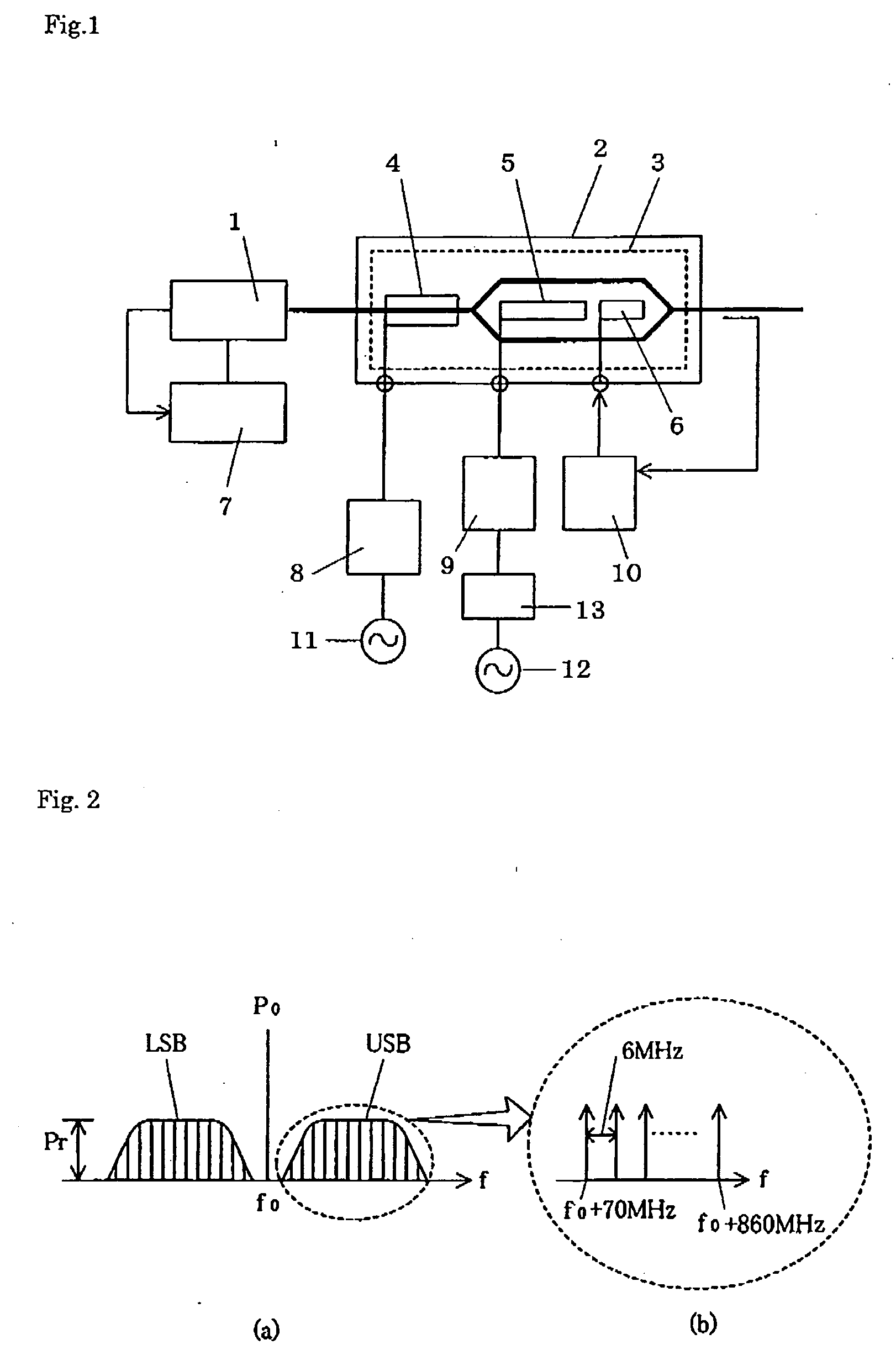
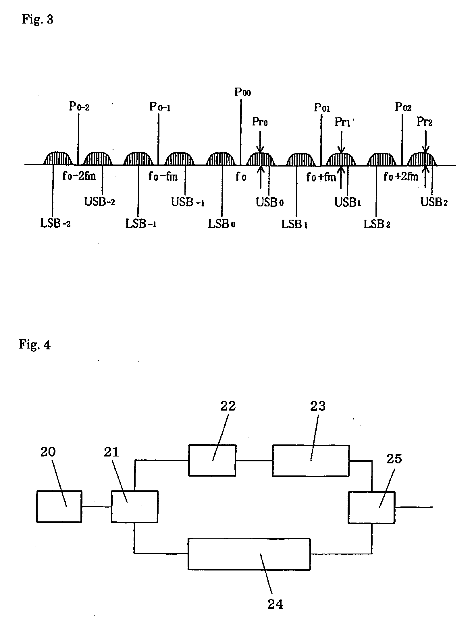
[0097] As shown in FIG. 6, an optical modulator according to the present invention includes a light branch means 30 for branching input light having the same carrier component as that of single mode light into two light waves, a SSB modulation means 31 for optically modulating one branched light wave and generating a light wave having the carrier component and one sideband spectrum, an intensity adjustment means 32 for adjusting a light intensity of the carrier component of the other branched light wave, a phase adjustment means 33 for adjusting the phase of the carrier component of at least one of the two branched light waves, and a multiplexing means 34 for multiplexing the two light waves passing through the SSB modulation means 31, the intensity adjustment means 32, and the phase adjustment means 33 to emit output light.

[0098] The light wave input to the optical modulator according t...


PUM


Abstract

An optical modulator which magnifies a modulation index and reduces affection of SBS by suppressing a light source carrier component in an equivalent light source spectral width and performs more long-distance transmission by suppressing one of sideband spectrums generated by a modulation signal to reduce affection of fiber dispersion, having a light branch means that branches input light having a carrier component into two light waves; a SSB modulation means that modulates one branched wave and generates a wave having the carrier component and one sideband spectrum; an intensity adjustment means that adjusts intensity of the carrier component of the other wave; a phase adjustment means that adjusts the phase of the carrier component with respect to at least one of the two waves; and a multiplexing means that multiplexes the two waves passing through the modulation means, and the intensity and phase adjustment means, and emits output light.

Description

BACKGROUND OF THE INVENTION [0001] (1) Field of the Invention [0002] The present invention relates to an optical modulator, and more particularly, to an optical modulator which can transmit a sub-carrier multiplexing (SCM) signal with a large output using an optical fiber. [0003] (2) Related Art Statement [0004] A broadcasting wave or a CATV wave is a SCM signal obtained by intensity-modulating a plurality of radio frequency (RF) carriers having an interval of 6 MHz based on a multi-channel (CH) video or audio signal. In order to transmit the SCM signal using an optical fiber, in a hybrid-fiber coaxial (HFC) system or a fiber-to-the-premise (FTTP) system, a direct modulation (DM) method of intensity-modulating light of a laser diode (LD) by the SCM signal according to the length of the fiber, the distribution number or the like, or an external modulation (EXT-M) method of intensity-modulating continuous light of a laser diode (LD) by the SCM signal using a lithium niobate (LN) modul...

Claims


Application Information

Patent Timeline
IPC IPC(8): G02F1/035H04B10/07H04B10/2507H04B10/2537H04B10/516H04B10/548H04B10/564H04B10/58H04B10/61
CPCG02F1/035G02F2001/212G02F1/225G02F1/212
Inventor SAKANE, TOSHIOMIYAZAKI, NORIKAZUHIGUMA, KAORUMORI, SHINGO
Owner SUMITOMO OSAKA CEMENT CO LTD
Why Eureka
Try Eureka