Light emission material and organic electroluminescent device using the same

Active Publication Date: 2006-12-21
TESCOM CORP
View PDF4 Cites 31 Cited by
  • Summary
  • Abstract
  • Description
  • Claims
  • Application Information

AI Technical Summary

Benefits of technology

[0009] It is therefore the object of the invention to provide an emission material and the organic electroluminescent device using the same. The emission material formed according to iridium and pyridyl-triazole ligand has the features of easy sublimation, quick response and high output rate and is capable of resolving the problems of difficult sublimation, poor he

Problems solved by technology

The Flrpic blue phosphorescent material is poor in sublimation, so temperature control during the purification process becomes a critical factor.
Moreover, the temperature of the Flrpic blue phosphorescent material during the sublimation and purification process is hard to control, so that the Fl

Method used


Image

  • Light emission material and organic electroluminescent device using the same
  • Light emission material and organic electroluminescent device using the same
  • Light emission material and organic electroluminescent device using the same

Examples


first embodiment

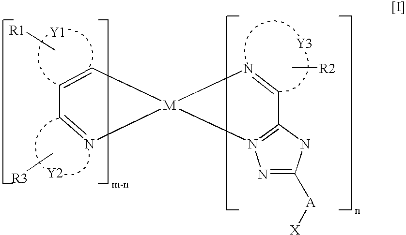
[0018] The invention provides an emission material having the features of easy sublimation, quick response and high output rate, therefore requires a shorter purification time than conventional Flrpic blue phosphorescent material. Compared with the conventional device using the Flrpic blue phosphorescent material, the device using the emission material of the invention obtains higher luminous efficiency and lower CIE value and has a bluer photochromism. The emission material of the invention is represented by chemical formula [I]:

[0019]“M” represents a metal atom whose atomic weight is greater than 40. m is smaller than or equal to the ligand number of “M”. n is a positive integral and is smaller than m. “Y1” is selected from aryl or heteroaryl. “Y2” and “Y3” are respectively selected from nitro-containing heterocyclic ring. “X”, “R1”, “R2” and “R3” are respectively selected from any substituent group or hydrogen. “A” is selected from aryl, heteroaryl or nitro-containing heterocyc...

second embodiment

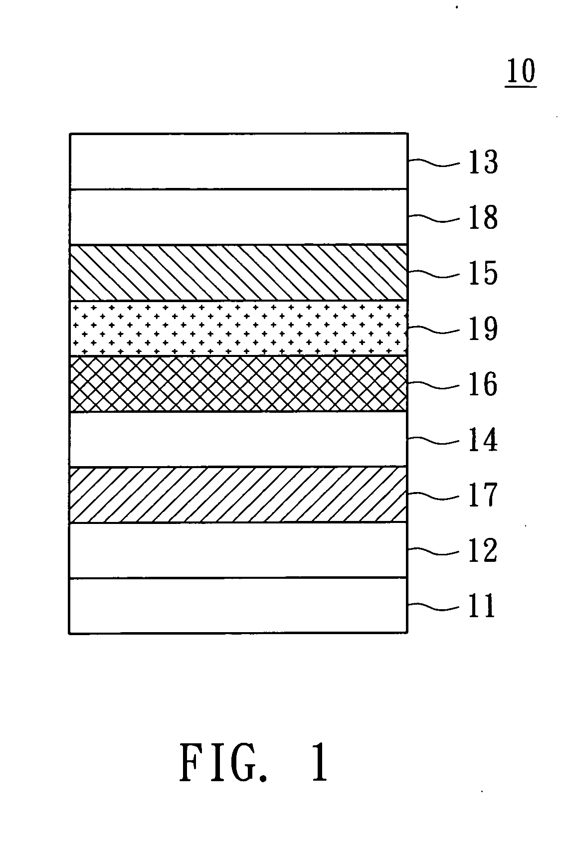
[0054] Referring to FIG. 1, a structural diagram of an OLED according to a second embodiment of the invention is shown. In the embodiment, the OELD, including organic light emitting diode (OLED) of small molecules and polymer light emitting diode (PLED), is exemplified by the OLED here. However, the technology disclosed in the embodiment is applicable to the PLED.

[0055] In FIG. 1, the OELD 10 includes a substrate 11, an anode 12, a cathode 13, a hole transport layer 14, an electron transport layer 15 and an emission layer 16. The anode 12 and the cathode 13 are disposed on the substrate 11. The hole transport layer 14 is disposed between the anode 12 and the cathode 13. The electron transport layer 15 is disposed between the hole transport layer 14 and the cathode 13. The emission layer 16 is disposed between the hole transport layer 14 and the electron transport layer 15, and the emission layer 16 includes a host and a dopant. The chemical structure of the dopant is represented by...

third embodiment

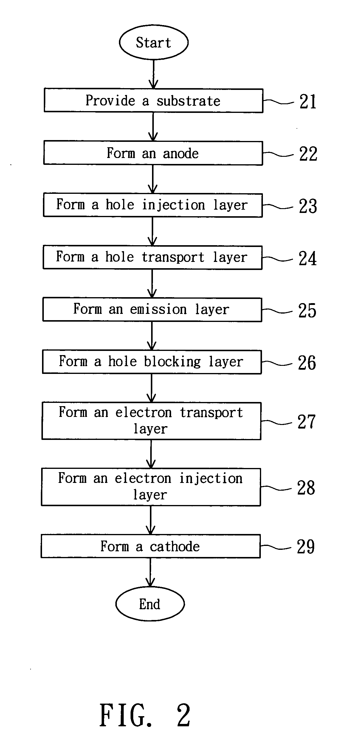
[0072] Referring to FIG. 2 is a flowchart of the manufacturing method of an OLED according to a third embodiment of the invention is shown. Refer to FIG. 1 at the same time. At first, the method begins at step 21, a substrate 11 is provided. Next, proceed to step 22, an anode 12 is formed on the substrate 11. Then, proceed to step 23, a hole injection layer 17 is formed on the anode 12. Next, proceed to step 24, a hole transport layer 14 is formed on the hole injection layer 17. Then, proceed to step 25, an emission layer 16 is formed on the hole transport layer 14. The emission layer 16 has a host and a dopant. The chemical structure of the dopant is represented by formulas [I]. Next, proceed to step 26, a hole blocking layer 19 is formed on the emission layer 16. Afterwards, proceed to step 27, an electron transport layer 15 is formed on the hole blocking layer 19. Next, proceed to step 28, an electron injection layer 18 is formed on the electron transport layer 15. At last, proce...


PUM

PropertyMeasurementUnit
Nanoscale particle sizeaaaaaaaaaa
Transport propertiesaaaaaaaaaa

Abstract

An organic electroluminescent device including a substrate, an anode, a cathode, a hole transport layer, an electron transport layer and an emission layer is provided. The anode and the cathode are disposed on the substrate. The hole transport layer is disposed between the anode and the cathode. The electron transport layer is disposed between the hole transport layer and the cathode. The emission layer is disposed between the hole transport layer and the electron transport layer. The chemical structure of the dopant is represented by formula [I]: “M” represents a metal atom, m is smaller than or equal to the ligand number of “M”, n is smaller than m. “Y1” is selected from aryl or heteroaryl. “Y2” and “Y3” are respectively selected from nitro-containing heterocyclic ring. “X”, “R1”, “R2” and “R3” are respectively selected from any substituent group or hydrogen. “A” is selected from aryl, heteroaryl or nitro-containing heterocyclic group.

Description

[0001] This application claims the benefit of Taiwan application Serial No. 94119903, filed Jun. 15, 2005, the subject matter of which is incorporated herein by reference. BACKGROUND OF THE INVENTION [0002] 1. Field of the Invention [0003] The invention relates in general to an emission material, and more particularly to a phosphorescent emission material and the organic electroluminescent device using the same. [0004] 2. Description of the Related Art [0005] In recent years, organic electroluminescent display has gained a rapid growth, and transition metal complex compounds are widely applied to the emission material. Take the emission layer for example, the emission material is categorized as fluorescent type and phosphorescent type. The luminous efficiency of the phosphorescent type is about three times as higher as that of the fluorescent type. The phosphorescence normally exists in the form of transition metal complex compounds. Due to the heavy-atom effect, intersystem crossin...

Claims


Application Information

Patent Timeline
IPC IPC(8): H01L51/54H05B33/14C09K11/06
CPCC09K11/06C09K2211/1007C09K2211/1029H05B33/14C09K2211/185H01L51/0085H01L51/5016C09K2211/1059Y10S428/917H10K85/342H10K50/11H10K2101/10
Inventor WU, PEI-CHI
Owner TESCOM CORP
Why Eureka
Try Eureka