Stacked annealing system

Inactive Publication Date: 2006-12-28
WAFERMASTERS
View PDF9 Cites 8 Cited by
  • Summary
  • Abstract
  • Description
  • Claims
  • Application Information

AI Technical Summary

Benefits of technology

[0011] The process chamber having two adjacently stacked cold and hot plates can be themselves stacked to create a low cost, simple vertical multi-wafer processing system having a small footprint. In another embodiment, N stacked cold plates and N stacked hot plates can be adjacently placed into a single process chamber so that N-1 wafers can be heated and cooled simultaneously, where N is greater than two.
[0012] Advantages of the present invention include more eff

Problems solved by technology

Other deposited layers (e.g., copper films) may have properties that undesirably change over time or “self-anneal”, resulting in unpredictable deposited layer properties (e.g., unpredictable resistivity, stress, grain size, and hardness).
Unfortunately, conventional lamp-based RTP systems have considerable drawbacks with regard to uniform tem

Method used


Image

  • Stacked annealing system
  • Stacked annealing system
  • Stacked annealing system

Examples


Embodiment Construction

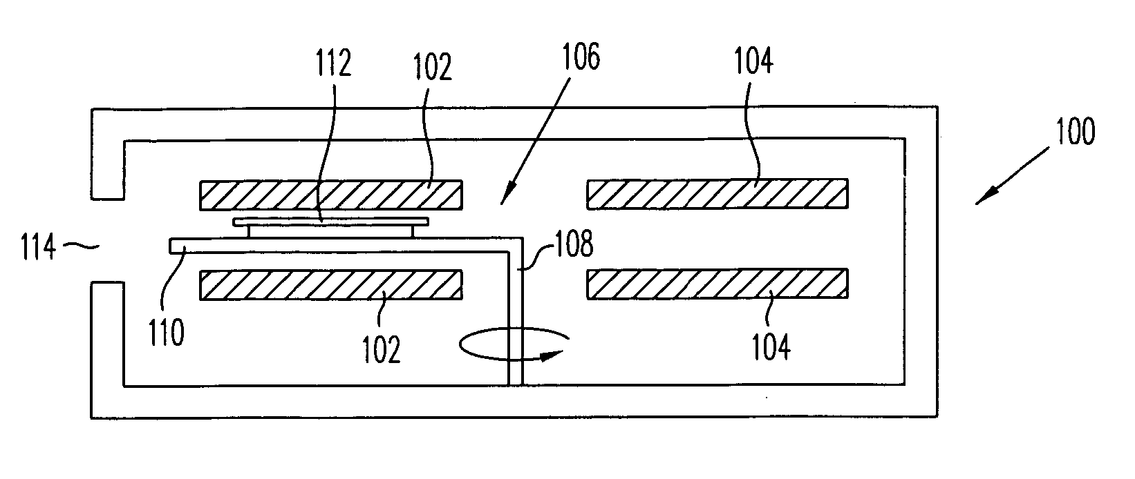
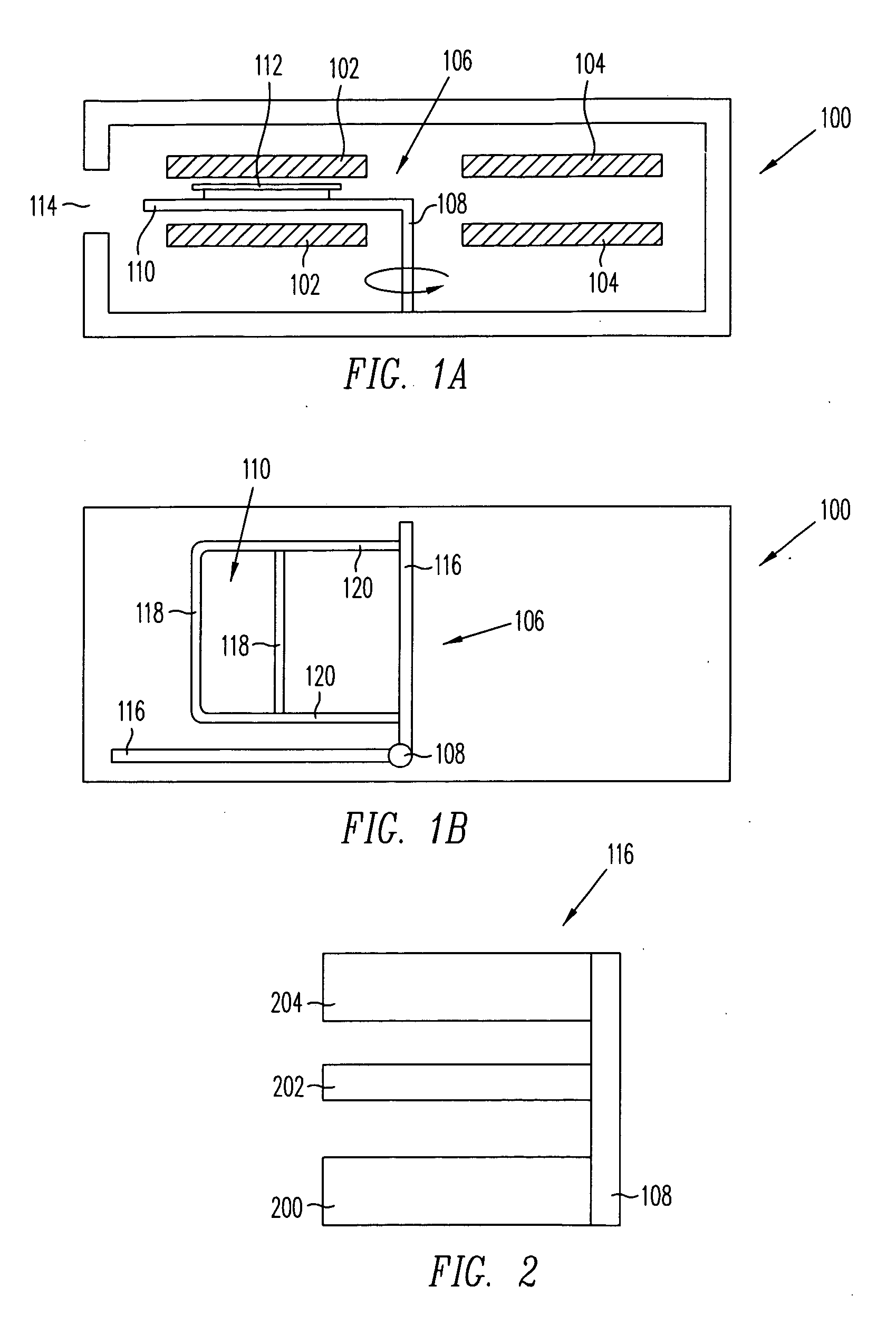
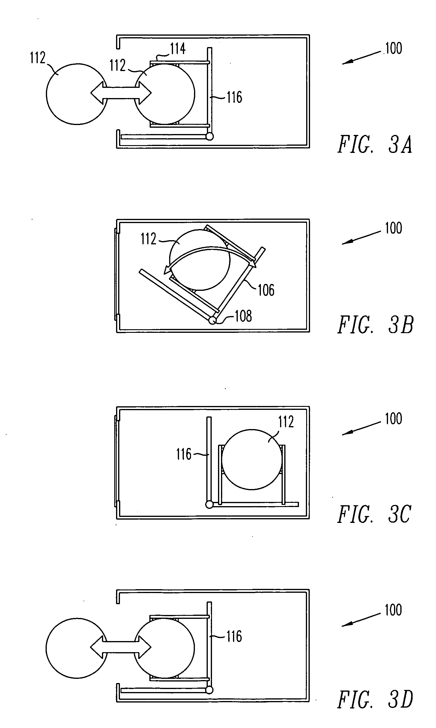
[0022]FIGS. 1A and 1B show side and top views, respectively, of a process chamber 100 according to one embodiment of the invention. Referring to FIG. 1A, chamber 100 includes two stacked cold plates 102 on one side and two stacked hot plates 104 on the other side. A rotatable wafer transport 106 is rotatable about a pivot or axis 108 between cold plates 102 and hot plates 104. Wafer transport 106 includes a wafer support 110 for holding a wafer 112, where the wafer that can be rotated between cold plates 102 and between hot plates 104. When wafer 112 is between cold plates 102, the wafer is cooled. When wafer 112 is rotated between hot plates 104, the wafer is heated to a desired temperature, such as for RTP or annealing. Chamber 100 includes an opening 114 to enable the wafer to be placed into and removed from chamber 100. Once the wafer is either inserted or removed from the chamber, the opening can be sealed, as is known in the art with conventional mechanisms.

[0023] Opening 114...


PUM

PropertyMeasurementUnit
Angleaaaaaaaaaa
Volumeaaaaaaaaaa

Abstract

A process chamber includes an opening, two or more stacked cold plates adjacent the opening, two or more stacked hot plates adjacent the cold plates, and a rotatable wafer transport capable of moving a wafer between the cold plates and between the hot plates for processing of the wafer. The wafer can be rapidly heated while between the hot plates. The wafer transport has perpendicular walls about a pivot such that when the wafer is between the cold plates or between the hot plates, one of the walls separates the cold and hot portions, thereby increasing the efficiency of cooling and heating.

Description

BACKGROUND [0001] 1. Field of the Invention [0002] The present invention relates generally to semiconductor wafer processing systems, and more particularly to such systems for the transfer of semiconductor wafers to a processing chamber. [0003] 2. Related Art [0004] High temperature processing of silicon wafers is important for manufacturing modern microelectronics devices. Such processes, including silicide formation, implant anneals, oxidation, diffusion drive-in and chemical vapor deposition (CVD), may be performed at high temperatures using conventional thermal processing techniques. Furthermore, many microelectronics circuits require feature sizes smaller than one micron and junction depths less than a few hundred angstroms. In order to limit both the lateral and downward diffusion of dopants, as well as to provide a greater degree of control during processing, it is desirable to minimize the duration of high temperature processing. [0005] Semiconductor wafers, flat panel displ...

Claims


Application Information

Patent Timeline
IPC IPC(8): A21B2/00F26B19/00
CPCH01L21/67109H01L21/67178H01L21/68764H01L21/67745H01L21/6719H01L21/324H01L21/02
Inventor YOO, WOO SIK
Owner WAFERMASTERS
Why Eureka
Try Eureka