Solid state membrane channel device for the measurement and characterization of atomic and molecular sized samples

a solid-state membrane channel and sample technology, applied in measurement devices, scientific instruments, instruments, etc., can solve the problems of tedious and laborious work, high cost of desired characterization of a particular polymer sequence, and large time and effort required to complete, etc., to achieve repeatable and highly accurate devices, facilitate longitudinal measurements, and precise conductive layers

Inactive Publication Date: 2006-12-28
ADVANCED RES
View PDF16 Cites 16 Cited by
  • Summary
  • Abstract
  • Description
  • Claims
  • Application Information

AI Technical Summary

Benefits of technology

[0011] In practice, it may be more practical to provide one or more dielectric layers that effectively protect and insulate the conductive layers. The use of such dielectric layers can simplify the manufacturing process and allows for multi-level conductive layering to be generated. That is, providing a single conductive layer or effectively providing electrical leads in a common plane allows for measurements of the particular polymer base in a transverse direction. However, by stacking conductive layers atop one another (electrically isolated from one another such as by an interposed dielectric layer), measurements of certain electrical characteristics can be taken in the longitudinal direction.
[0015] By utilizing dielectric layers, electrically conductive leads can be fabricated in multiple planes. This not only allows for transverse measurements to be made, but facilitates longitudinal measurements as well. Any configuration or variation of the single plane lead structures can be repeated with the multi-level thin film layers. Namely, relatively precise conductive layers can be applied relying on the focused ion beam or other precision cutting device to bisect each respective layer. Alternatively, a focused ion beam or other precision cutting device can be utilized for removing a precise amount of the electrically conductive layer in and around the desired channel area, once again resulting in any number of leads being fabricated in any given plane. Thus, multiple transverse and multiple longitudinal measurements can be made between any given pair of leads.
[0016] Longitudinal measurements in and of themselves may be sufficient to determine the necessary characteristics in the polymer material in question. That is, it is not necessary to have electrically isolated lead pairs in a single plane. This allows for an embodiment where a relatively imprecise electrically conductive layer is formed in a first plane. A second relatively imprecise electrically conductive layer is formed in a second plane wherein the second plane is separated from the first by a dielectric layer. By providing a nano-scale aperture through the entirety of the thin film layer (i.e., the dielectric layers and both the conductive layers), a completed structure is fabricated. In this embodiment, electrical measurements are not possible within a single plane. However, by measuring across different planar levels sufficient information may be gathered to characterize the polymer molecule. This configuration provides for relative ease during the manufacturing process and results in a repeatable and highly accurate device.

Problems solved by technology

This is generally tedious and laborious work and requires a significant amount of time and effort to complete.
Thus, the results from any desired characterization of a particular polymer sequence are usually quite expensive and take a fair amount of time to obtain.
The drawback of this device is that it is difficult to create an impermeable membrane having a sufficiently small ion channel that will allow the device to function properly.
This is extremely difficult to do on a cost effective and repetitive scale.
Specifically, the formation of an otherwise impermeable organic membrane and chemically etching or otherwise forming the ion channel is a hit or miss operation that may or may not actually produce the appropriately channeled membrane.
Thus, while the concept of providing for the rapid determination of the character of polymer molecules is an extremely important one, no device has been provided that can be reliably produced while achieving accurate results.

Method used


Image

  • Solid state membrane channel device for the measurement and characterization of atomic and molecular sized samples
  • Solid state membrane channel device for the measurement and characterization of atomic and molecular sized samples
  • Solid state membrane channel device for the measurement and characterization of atomic and molecular sized samples

Examples


Embodiment Construction

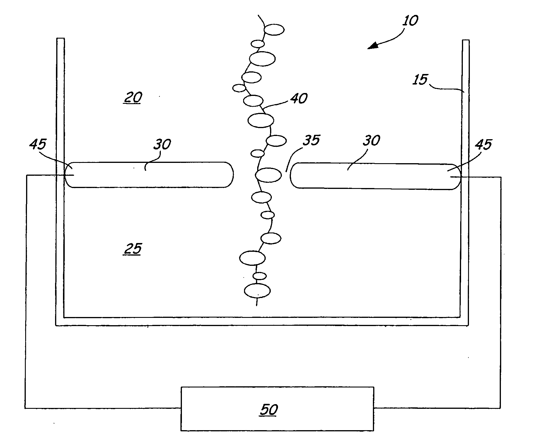
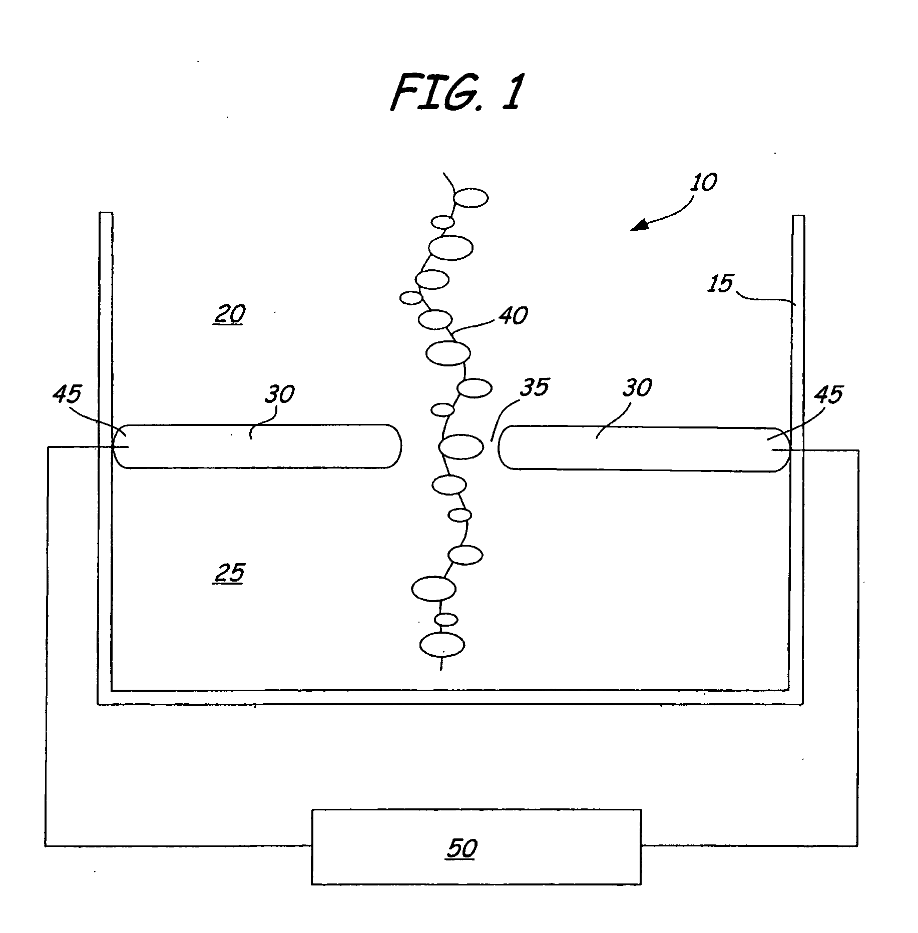
[0040] Referring to FIG. 1, a channel device is illustrated and generally referred to as 10. Channel device 10 includes container 15 within which resides a volume of fluid. The fluid is separated into an upper pool 20 and lower pool 25 by a membrane 30. The liquid within upper pool 20 and lower pool 25 is preferably a conductive solution and contains a number of linear polymer molecules 40. Polymer molecules 40 are free to travel through the liquid medium contained within container 15. FIG. 1 is provided for illustrative purposes only and the components shown are not drawn to scale in general or with respect to each other.

[0041] By using various processes, such as introducing a voltage differential across membrane 30, polymer molecules 40 can be directed through channel 35 in membrane 30. Channel 35 is a nano-scale aperture. Typically, channel 35 will have a diameter of up to about 10 nm and preferably between 2-4 mn. Of course, the actual size will be selected to best serve the de...


PUM

PropertyMeasurementUnit
diameteraaaaaaaaaa
diameteraaaaaaaaaa
thicknessaaaaaaaaaa

Abstract

The present invention relates to an apparatus for characterization of molecules through measurement of various electrical characteristics. The apparatus has a substrate on which is formed a thin film layer. Further, the apparatus has an insulation layer formed on the thin film layer. The thin film layer has a defined channel bored therethrough, the substrate has an aperture bored therethrough, and the insulation layer has a hole formed therethrough.

Description

CROSS-REFERENCE TO RELATED APPLICATION(S) [0001] This application claims priority to Provisional Application 60 / 549,614, filed on Mar. 2, 2004, which is incorporated herein by reference in its entirety. This application further claims priority as a continuation-in-part of U.S. patent application Ser. No. 10 / 656,859, filed on Sep. 5, 2003, which is a continuation of U.S. patent application Ser. No. 09 / 815,461, which was filed on Mar. 23, 2001 and issued as U.S. Pat. No. 6,616,895 on Sep. 9, 2003, which claims priority to Provisional Application Ser. No. 60 / 191,663, filed Mar. 23, 2000, all of which are incorporated herein by reference in their entirety. This application also claims priority as a continuation-in-part of U.S. patent application Ser. No. 10 / 685,289, filed on Oct. 14, 2003, which claims priority to Provisional Application Ser. No. 60 / 418,507, filed on Oct. 15, 2002 and Provisional Application Ser. No. 60 / 191,663, filed on Mar. 23, 2000, all of which are incorporated here...

Claims


Application Information

Patent Timeline
Patent Type & Authority Applications(United States)
IPC IPC(8): G01N33/00
CPCG01N33/48721
Inventor DUGAS, MATTHEW P.ZIELINSKI, BRANT W.
Owner ADVANCED RES
Why Eureka
Try Eureka