Method of producing a semiconductor device with an aluminum or aluminum alloy electrode

a technology of aluminum alloy and semiconductor devices, applied in the direction of semiconductor devices, electrical equipment, transistors, etc., can solve the problems of unfavorable leakage current generation, loss of device function, and high cost of the epitaxial substrate, and achieve the effect of avoiding the generation of aluminum spikes

Inactive Publication Date: 2007-01-04
FUJI ELECTRIC CO LTD
View PDF5 Cites 19 Cited by
  • Summary
  • Abstract
  • Description
  • Claims
  • Application Information

AI Technical Summary

Benefits of technology

[0022] In the case of producing a reverse blocking IGBT, a film of aluminum or an aluminum alloy having a thickness of at least 0.3 μm is formed in contact with the collector layer for a rear electrode. A silicon concentration in the aluminum alloy film need not be specified. When the aluminum alloy film is thinner than 0.3 μm, say about 0.1 μm, the rear electrode can be composed of an aluminum alloy film with a silicon concentration of 2 percent by weight or more in contact with the collector layer. This measure can be applied to an FS type IGBT. The method of the invention prevents generation of aluminum spi...

Problems solved by technology

Moreover, the epitaxial substrate is costly.
Because the PN junction in these devices is located at a shallow depth of about 0.3 μm in the rear surface region, a small flaw in the rear surface region can cause a punch-through phenomenon leading to loss of device function.
If a spike 11 reaches a buffer layer 10 in an FS type IGBT, unfavorable leakage current results.
If a spike 11 reaches a PN junction in a reverse blocking type IGBT, insufficient reverse withstand voltage and unfavorable reverse leakage...

Method used


Image

  • Method of producing a semiconductor device with an aluminum or aluminum alloy electrode
  • Method of producing a semiconductor device with an aluminum or aluminum alloy electrode
  • Method of producing a semiconductor device with an aluminum or aluminum alloy electrode

Examples


first embodiment

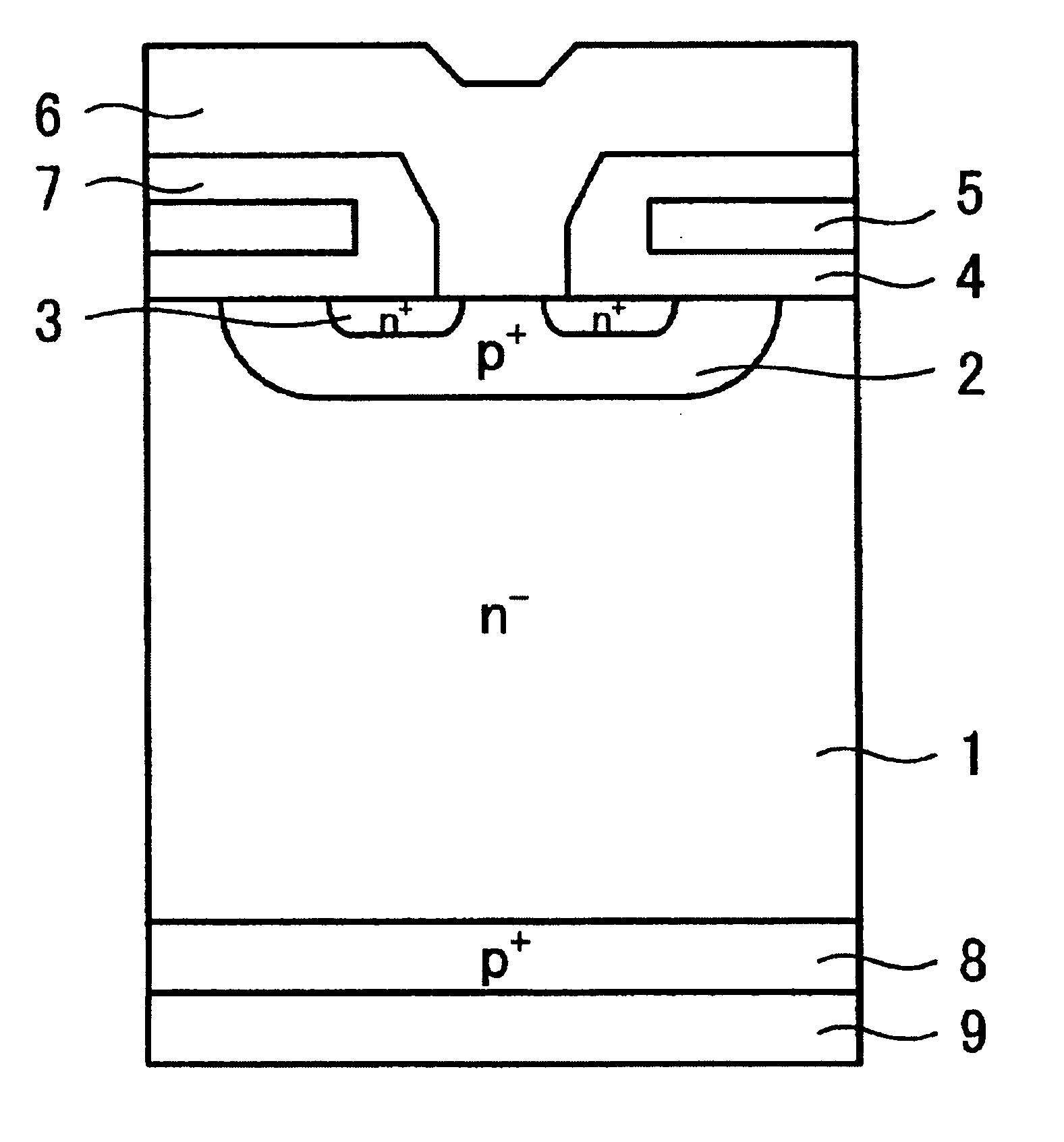
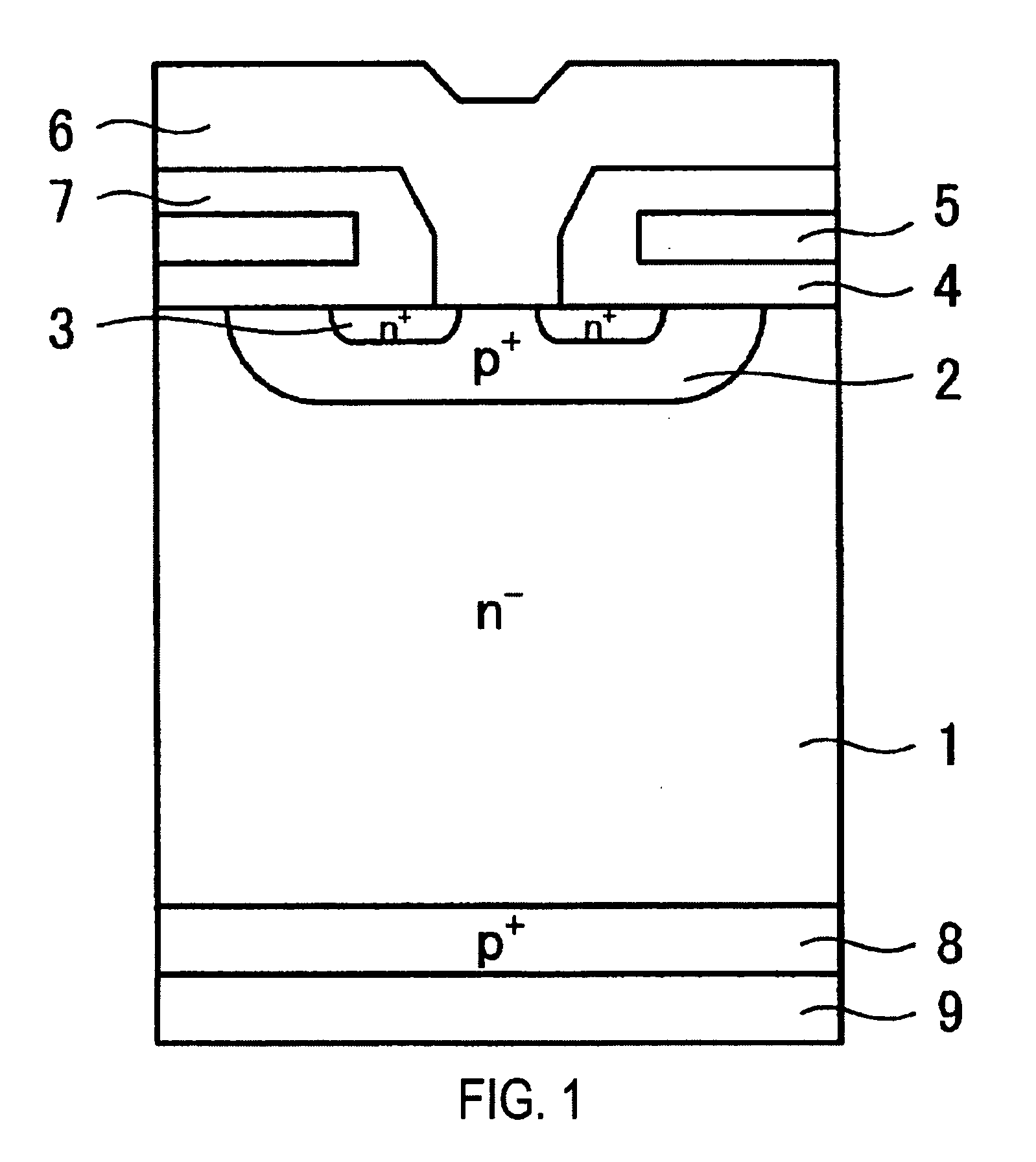
[0050]FIG. 2 and FIG. 4 through 8 are sectional views illustrating a method of producing an FS type IGBT according to the invention. Referring to FIG. 2 and FIG. 4, in the front surface region of an n− FZ substrate (FZ-N), which Works as an active layer (a drift layer) 1, a front surface region device structure 12 is first formed consisting of a base region, an emitter region, a gate oxide film, a gate electrode, an interlayer insulation film, an emitter electrode, and an insulation protective film (omitted in FIG. 2).

[0051] The gate oxide film may be made of silicon oxide (SiO2), for example. The gate electrode may be made of polysilicon, for example. The interlayer insulation film may be made of BPSG, for example. The emitter electrode may be made of aluminum-silicon, for example. The aluminum-silicon film is heat treated at a relatively low temperature in the range of 350° C. to 450° C. in order to obtain a low resistance wiring with stable joining ability. The insulation protec...

second embodiment

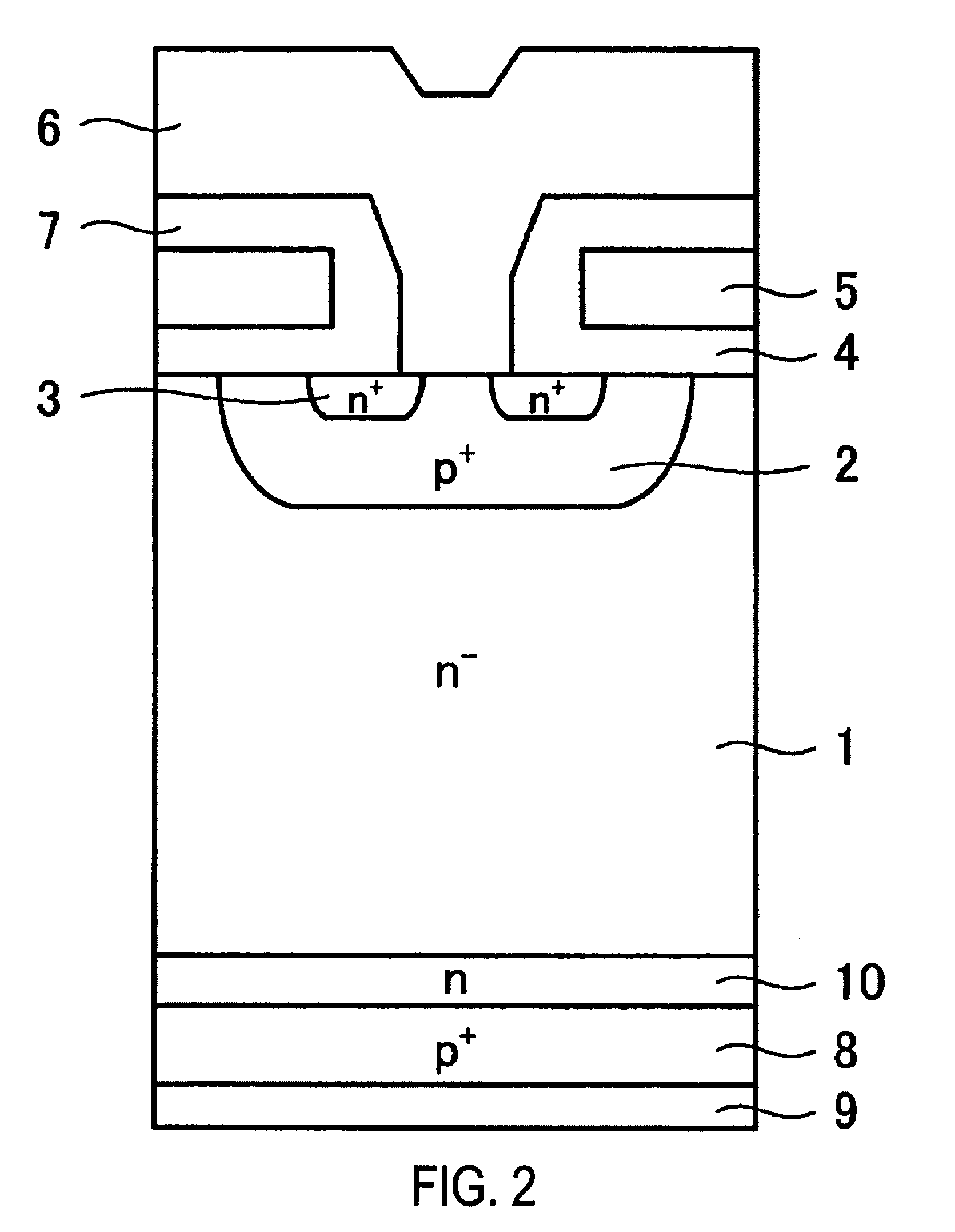
[0059]FIGS. 11 through 14 are sectional views illustrating a method of manufacturing a reverse blocking IGBT according to the present invention. Referring to FIG. 11, a p type isolation region 15 is first formed in an n− FZ substrate that works as an active layer (a drift layer) 1 by selective thermal diffusion of p type ions from above. To produce a device of a rating voltage of 1,200 V, the p type ions are diffused to a depth of about 200 μm.

[0060] Subsequently, as shown in FIG. 12, a front surface side device structure is formed in the surface region of the FZ substrate surrounded by the isolation region 15, the device structure being composed of a base region 2, an emitter region 3, a gate oxide film 4, a gate electrode 5, an interlayer insulation film 7, and emitter electrode 6, and an insulation protective film (not shown in the figure). Then, the rear surface of the substrate is ground by back grinding or the like, until the isolation region 15 is exposed as indicated by a d...


PUM


Abstract

A method of producing a semiconductor device having a thickness of 90 μm to 200 μm and with an electrode on the rear surface, which achieves a high proportion of non-defective devices by optimizing the silicon concentration and thickness of the aluminum-silicon electrode. A surface device structure is formed on a first major surface of a silicon substrate. A buffer layer and a collector layer are formed on the second major surface after grinding to reduce the thickness of the substrate. On the collector layer, a collector electrode is formed including a first layer of an aluminum-silicon film having a thickness of 0.3 μm to 1.0 μm and a silicon concentration of 0.5 percent to 2 percent by weight, preferably not more than 1 percent by weight.

Description

CROSS-REFERENCE TO RELATED APPLICATION [0001] This application is based on, and claims priority to, Japanese Patent Application No. 2005-179720, filed on Jun. 20, 2005, the contents of which are incorporated herein by reference. BACKGROUND OF THE INVENTION [0002] 1. Field of the Invention [0003] The present invention relates to a method of producing a semiconductor device, in particular, a power semiconductor device that can be applied to power conversion apparatuses, has a thickness between 90 to 200 μm, and is provided with an electrode on the rear surface of the device. [0004] 2. Description of Related Art [0005] An IGBT (insulated gate bipolar transistor), a type of power semiconductor device, is a one-chip power device that gives a high speed switching characteristic and voltage-driving ability, which are specialties of MOSFETs (or insulated gate type field effect transistors), and a low forward voltage drop characteristic, which is a specialty of bipolar transistors. Applicati...

Claims


Application Information

Patent Timeline
IPC IPC(8): H01L21/20
CPCH01L29/0834H01L29/41725H01L29/7393H01L29/66333H01L29/7395H01L29/456
Inventor KAZAMA, KENICHINAKAJIMA, TSUNEHIROSASAKI, KOJISHIMIZU, AKIOHAYASHI, TAKASHIWAKIMOTO, HIROKI
Owner FUJI ELECTRIC CO LTD
Why Eureka
Try Eureka