Semiconductor device and method of manufacturing semiconductor device

a semiconductor and semiconductor technology, applied in the direction of semiconductor devices, electrical equipment, basic electric elements, etc., can solve the problems of uniform width of a fin formed by using the silicon nitride film as a mask, inability to easily ensure the selectivity between the hard mask and the photoresist mask and the silicon nitride film, and deterioration of the side wall of the patterned silicon nitride film

Active Publication Date: 2007-01-04
MICROSOFT TECH LICENSING LLC
View PDF4 Cites 111 Cited by
  • Summary
  • Abstract
  • Description
  • Claims
  • Application Information

AI Technical Summary

Benefits of technology

[0011] A semiconductor device according to an embodiment of the invention comprises an insulation layer; a plurality of Fins arranged on the insulating film at a pitch smaller than a minimum pitch which can be achieved by lithography; gate insulation films formed on sidewalls of the Fins; a gate electrode which extends in a direction of arrangement of the Fins and which is electrically insul

Problems solved by technology

More specifically, in this case, selectivity between both the hard mask and the photoresist mask and the silicon nitride film cannot be easily assured.
More specifically, the verticality of the side wall of the patterned silicon nitride film is deteriorated.
In this manner, the width of a Fin formed by using the sil

Method used


Image

  • Semiconductor device and method of manufacturing semiconductor device
  • Semiconductor device and method of manufacturing semiconductor device
  • Semiconductor device and method of manufacturing semiconductor device

Examples


first embodiment

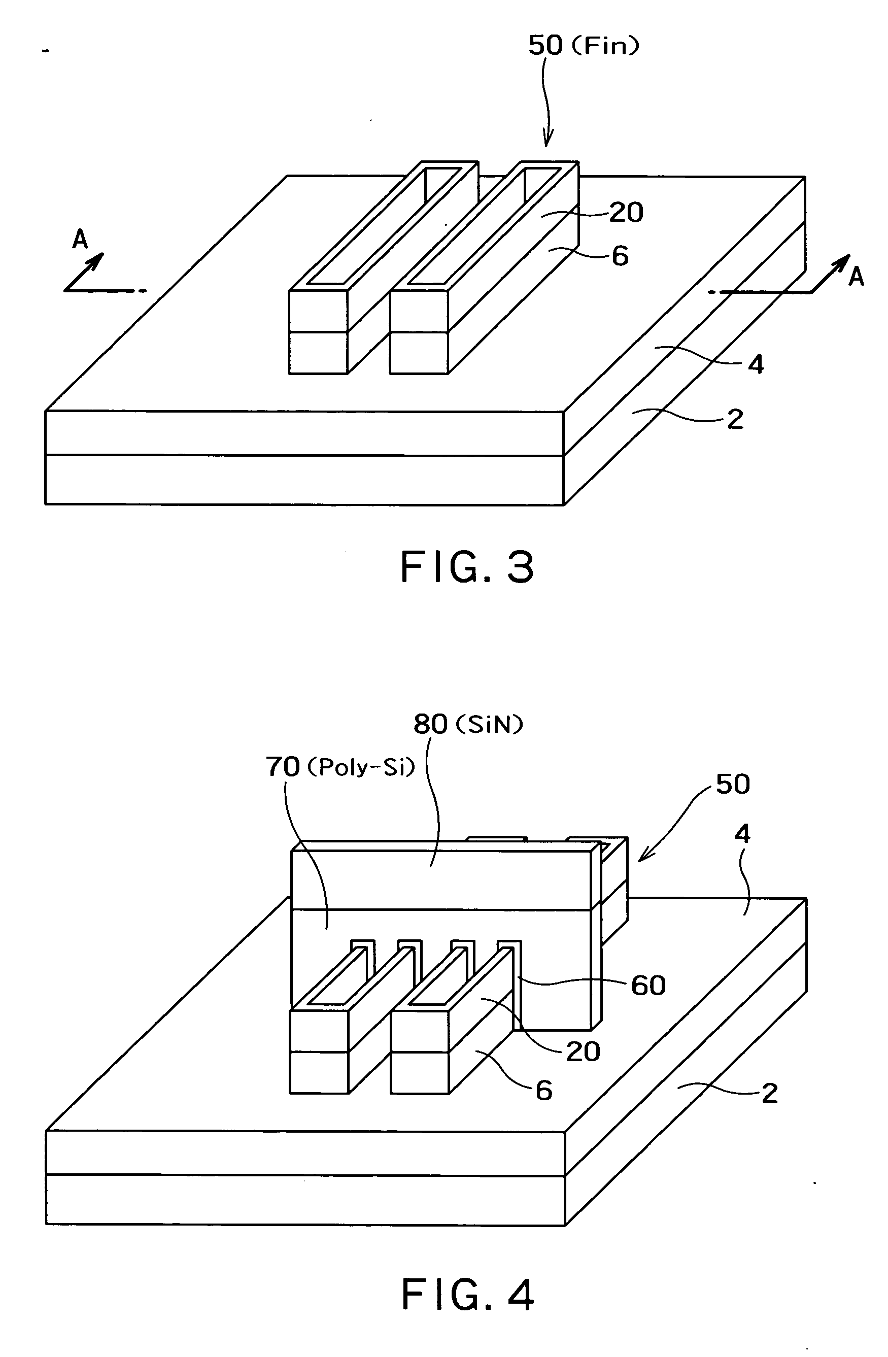
[0019] FIGS. 1 to 7 are diagram showing a method of manufacturing a Fin FET according to the first embodiment of the present invention. FIGS. 1 and 2 are sectional views, and FIGS. 3 to 7 are perspective views.

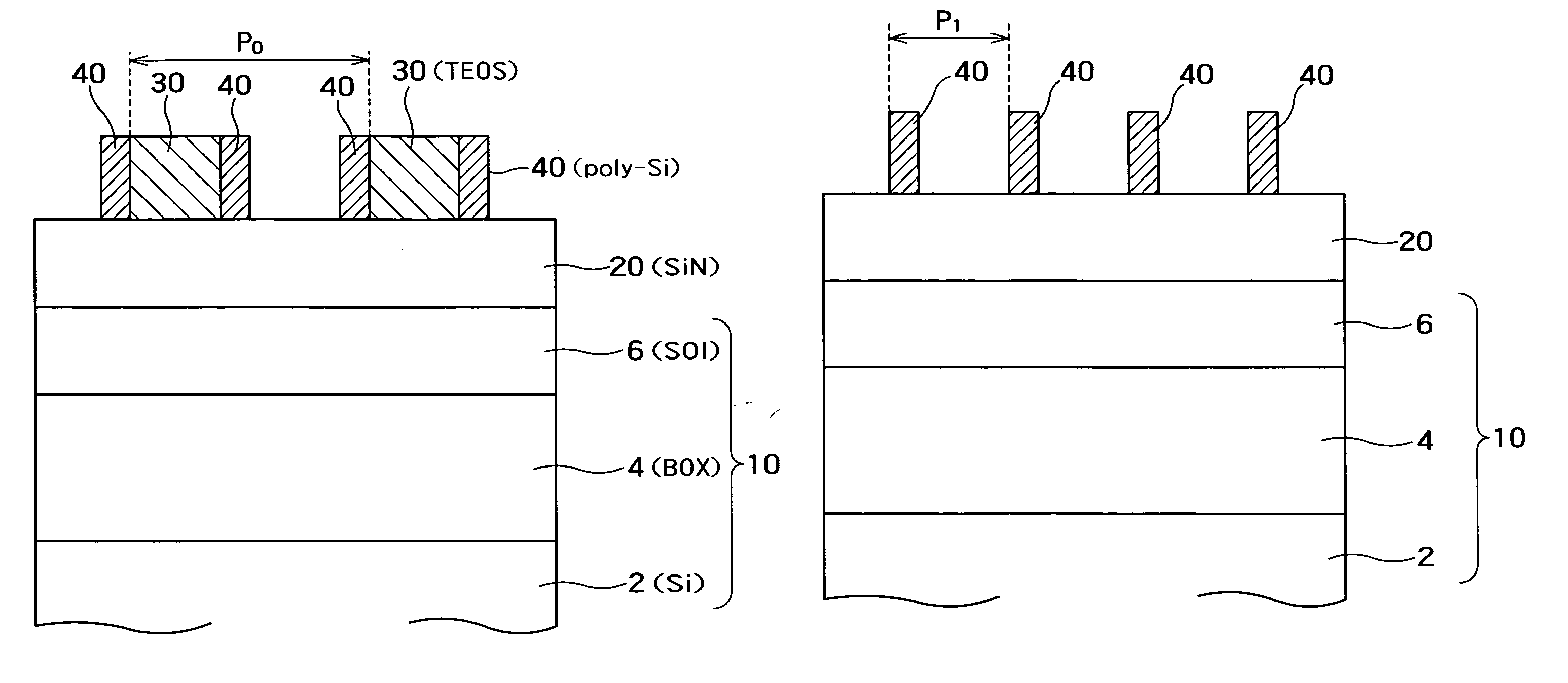
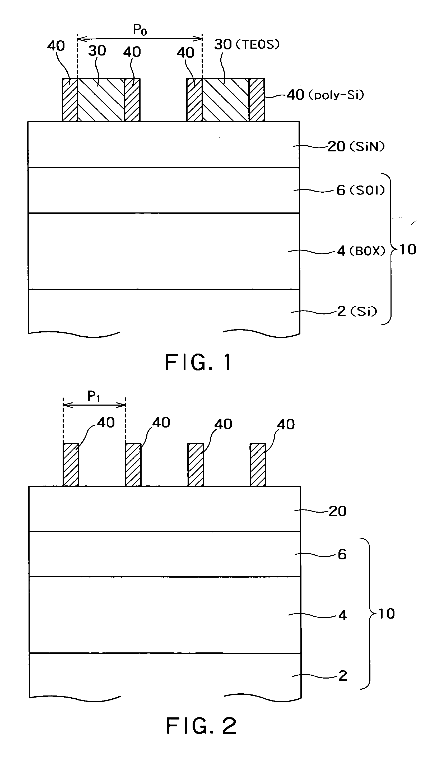
[0020] As shown in FIG. 1, an SOI substrate 10 including a silicon substrate 2, a BOX (Buried Oxide) layer 4, and an SOI layer 6 is prepared. The thickness of the SOI layer 6 is about 50 nm. A silicon nitride film 20 is deposited on the SOI layer 6 as a material for a hard mask. The width of the silicon nitride film 20 is about 70 nm.

[0021] A TEOS (tetraethoxysilane) film for a dummy pattern is deposited on the silicon nitride film 20. The thickness of the TEOS film is about 100 nm. The TEOS film is patterned by a lithography technique to form a dummy pattern 30. A plurality of dummy patterns 30 are formed to be arranged at a minimum pitch P0 which can be achieved by lithography. In FIG. 1, two dummy patterns 30 are shown. However, patterning may be performed to arrange thre...

second embodiment

[0041] FIGS. 10 to 12 are perspective views showing a method of manufacturing a Fin FET according to the second embodiment of the present invention. The second embodiment is different from the first embodiment in the step of forming a source-drain region. Therefore, in the second embodiment, the Fin FET is formed by the same method as in the first embodiment until the step shown in FIG. 5.

[0042] As shown in FIG. 10, a silicon oxide film 140 is deposited by an HDP (High Density Plasma)-CVD method to cover the Fins 50. The thickness of the silicon oxide film 140 is about 400 nm. After the silicon oxide film 140 is planarized by CMP, the silicon oxide film 140 is etched back by hydrofluoric acid or the like until the hard mask 80 on the gate electrode 70 is exposed. Then, the hard mask 80 is wet-etched to expose the top surface of the gate electrode 70. A metal, e.g., nickel is deposited on the gate electrode 70. The nickel is subjected to heat treatment to fully silicide the gate ele...

third embodiment

[0049]FIG. 13 is a perspective view of a Fin FET according to an embodiment of the present invention. An SOI substrate is used in the first and second embodiments. However, a bulk silicon substrate 3 is used in the third embodiment. Therefore, a silicon nitride film 20 for a hard mask is deposited on the bulk silicon substrate 3. SWT or multi-SWT is applied to the silicon nitride film 20 to form a hard mask having a pitch smaller than the minimum pitch P0 which can be achieved by lithography. The dummy pattern 30 is etched by RIE using the hard mask. In this manner, Fins 50 having a pitch smaller than the pitch P0 are formed. At this time, a trench is formed between the Fins 50. A silicon oxide film 5 is filled in a lower part of the trench. In this manner, STI (Shallow Trench Isolation) is formed. Since no silicon oxide film is deposited on the upper part of the trench, a structure in which the Fins 50 project on the silicon oxide film 5 as shown in FIG. 13.

[0050] Thereafter, a Fi...


PUM


Abstract

A method of manufacturing a semiconductor device includes forming a plurality of Fins including a semiconductor material on an insulation layer; forming gate insulation films on sidewalls of the Fins; forming a gate electrode which extends in a direction of arrangement of the Fins and which is electrically insulated from the Fins, the gate electrode is common in the Fins on the gate insulation film; implanting an impurity into portions of the Fins by using the gate electrode as a mask to form a source-drain diffusion layer, the portions of the Fins extending on both sides of the gate electrodes; and depositing a conductive material on both sides of the Fins to connect the Fins to each other.

Description

CROSS-REFERENCE TO RELATED APPLICATION [0001] This application is based upon and claims the benefit of priority from the prior Japanese Patent Applications No. 2005-173606, filed on Jun. 14, 2005, the entire contents of which are incorporated herein by reference. BACKGROUND OF THE INVENTION [0002] 1. Field of the Invention [0003] The present invention relates to a semiconductor device and a method of manufacturing a semiconductor device. [0004] 2. Related Art [0005] As a method of forming a Fin portion of a Fin transistor, a spacer-lithography technique is proposed. As the spacer-lithography technique, a Sidewall pattern Transfer (SWT) technique is known. [0006] The SWT is a method which can form Fin portions at a pitch smaller than the minimum pitch of lithography. Conventional SWT is executed by the following method. A silicon nitride film is deposited on an SOI (Silicon On Insulator). Furthermore, in a region for forming a Fin, a hard mask such as a TEOS film on poly-Si film is f...

Claims


Application Information

Patent Timeline
IPC IPC(8): H01L21/8234H01L21/336
CPCH01L21/845H01L27/1211H01L2029/7858H01L29/66795H01L29/785H01L29/41791
Inventor YAGISHITA, ATSUSHI
Owner MICROSOFT TECH LICENSING LLC
Why Eureka
Try Eureka