Method and apparatus for forming silicon oxynitride film

Inactive Publication Date: 2007-01-11
TOKYO ELECTRON LTD
View PDF3 Cites 70 Cited by
  • Summary
  • Abstract
  • Description
  • Claims
  • Application Information

AI Technical Summary

Benefits of technology

[0008] An object of the present invention is to provide a method and apparatus for forming a silicon ox

Problems solved by technology

For example, Jpn. Pat. Appln. KOKAI Publication No. 2004-281853 (Patent Document 1) discloses a method of forming a silicon nitride film by

Method used


Image

  • Method and apparatus for forming silicon oxynitride film
  • Method and apparatus for forming silicon oxynitride film
  • Method and apparatus for forming silicon oxynitride film

Examples


Embodiment Construction

[0046] An embodiment of the present invention will now be described with reference to the accompanying drawings. In the following description, the constituent elements having substantially the same function and arrangement are denoted by the same reference numerals, and a repetitive description will be made only when necessary.

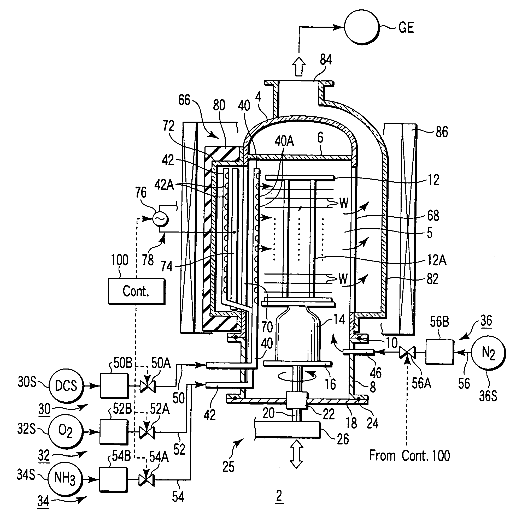
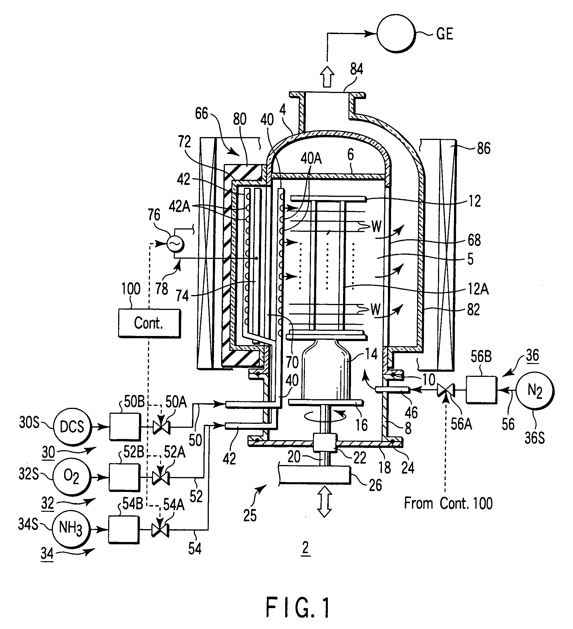
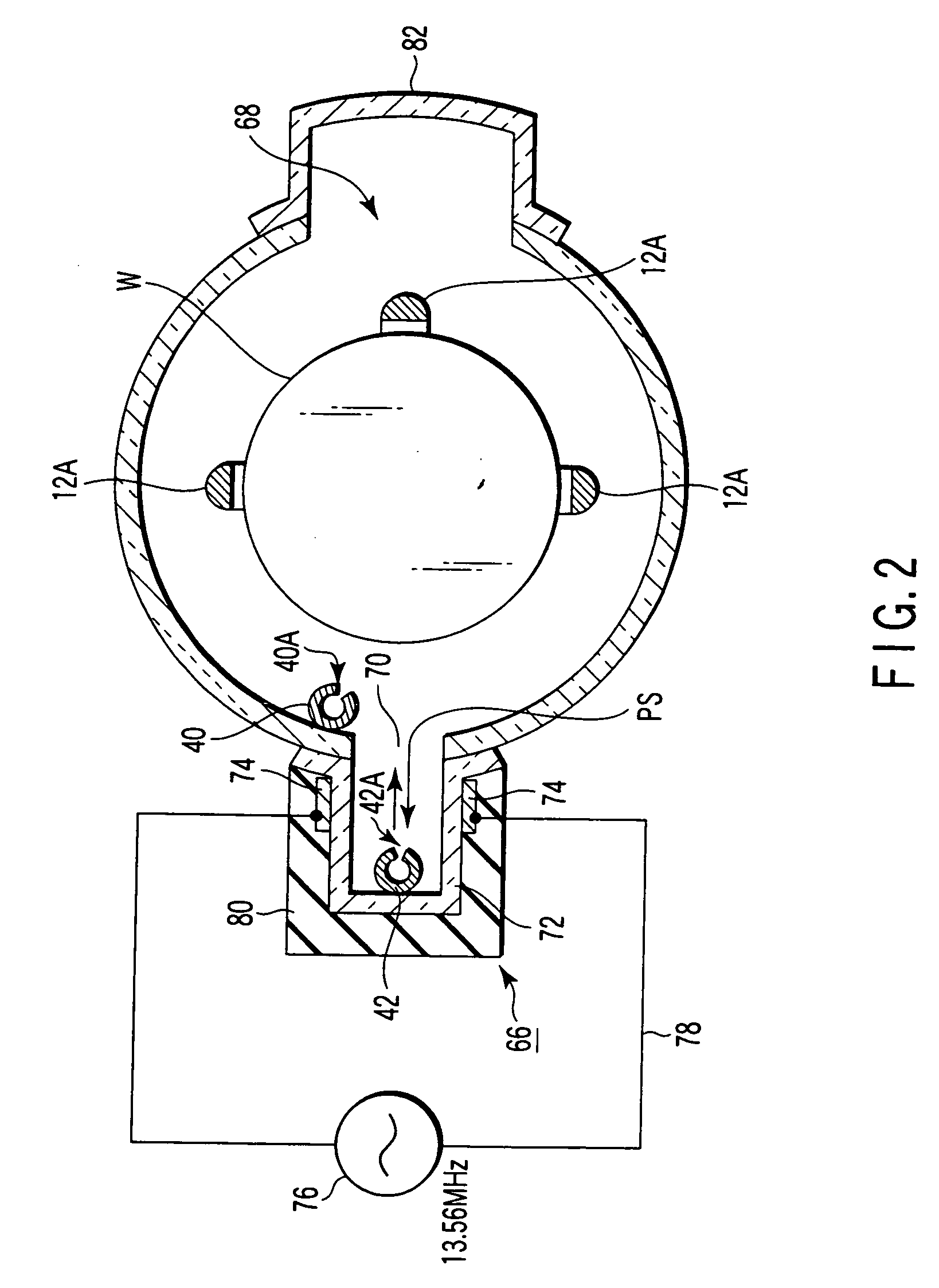
[0047]FIG. 1 is a sectional view showing a film formation apparatus (vertical CVD apparatus) according to an embodiment of the present invention. FIG. 2 is a sectional plan view showing part of the apparatus shown in FIG. 1. The film formation apparatus 2 has a process field configured to be selectively supplied with a first process gas containing dichlorosilane (DCS: SiH2Cl2) gas as a chlorosilane family gas, a second process gas containing oxygen (O2) gas as an oxidizing gas, and a third process gas containing ammonia (NH3) gas as a nitriding gas. The film formation apparatus 2 is configured to form a silicon oxynitride film on target substrates by CVD in t...


PUM

PropertyMeasurementUnit
Temperatureaaaaaaaaaa
Pressureaaaaaaaaaa
Pressureaaaaaaaaaa

Abstract

A silicon oxynitride film is formed on a target substrate by CVD, in a process field configured to be selectively supplied with a first process gas containing a chlorosilane family gas, a second process gas containing an oxidizing gas, and a third process gas containing a nitriding gas. This method alternately includes first to sixth steps. The first, third, and fifth steps perform supply of the first, second, and third process gases, respectively, while stopping supply of the other two process gases. Each of the second, fourth, and sixth steps stops supply of the first to third process gases. The third and fifth steps include an excitation period of supplying the second and third process gases, respectively, to the process field while exciting the respective process gases by an exciting mechanism.

Description

CROSS-REFERENCE TO RELATED APPLICATIONS [0001] This application is based upon and claims the benefit of priority from prior Japanese Patent Application No. 2005-197283, filed Jul. 6, 2005, the entire contents of which are incorporated herein by reference. BACKGROUND OF THE INVENTION [0002] 1. Field of the Invention [0003] The present invention relates to a film formation method and apparatus for a semiconductor process for forming a silicon oxynitride film on a target substrate, such as a semiconductor wafer. The term “semiconductor process” used herein includes various kinds of processes which are performed to manufacture a semiconductor device or a structure having wiring layers, electrodes, and the like to be connected to a semiconductor device, on a target substrate, such as a semiconductor wafer or a glass substrate used for an LCD (Liquid Crystal Display) or FPD (Flat Panel Display), by forming semiconductor layers, insulating layers, and conductive layers in predetermined pat...

Claims


Application Information

Patent Timeline
IPC IPC(8): C23C16/00G06F19/00H01L21/20B05C11/00C23C16/42H01L21/31H01L21/318
CPCC23C16/345H01L21/3145H01L21/3141C23C16/45546H01L21/0214H01L21/0228H01L21/02211C23C16/308C23C16/45527C23C16/45553
Inventor MATSUURA, HIROYUKI
Owner TOKYO ELECTRON LTD
Why Eureka
Try Eureka