Optically pumped semiconductor laser

a semiconductor laser and optical pump technology, applied in the direction of lasers, semiconductor lasers, optical resonator shape and construction, etc., can solve the problems of difficult miniaturization of the system, inability to reduce the distance between the pumping light source and the epitaxy structure, etc., to achieve the effect of miniaturizing the structure of the optical pumping semiconductor laser

Inactive Publication Date: 2007-01-18
SAMSUNG ELECTRONICS CO LTD
View PDF15 Cites 17 Cited by
  • Summary
  • Abstract
  • Description
  • Claims
  • Application Information

AI Technical Summary

Benefits of technology

[0012] One aspect of the present invention is to provide an optically pumped semiconductor laser and an optical pumping method capable of miniaturizing the structure of the optically pumped semiconductor laser.

Problems solved by technology

While the method of '318 patent can obtain a high output of second harmonic generation using a focusing lens and a nonlinear crystal, it is impossible to reduce a distance between a pumping light source and epitaxy structure as the focusing lens blocks infrared light as the pumping light source comes close to the epitaxy structure.
Therefore, the method of '318 patent is capable of generating a high output of laser, but it is difficult to miniaturize the system.

Method used


Image

  • Optically pumped semiconductor laser
  • Optically pumped semiconductor laser
  • Optically pumped semiconductor laser

Examples


Embodiment Construction

[0045] Hereinafter, the detailed description of an exemplary embodiment in accordance with the present invention will be apparent in connection with the accompanying drawings.

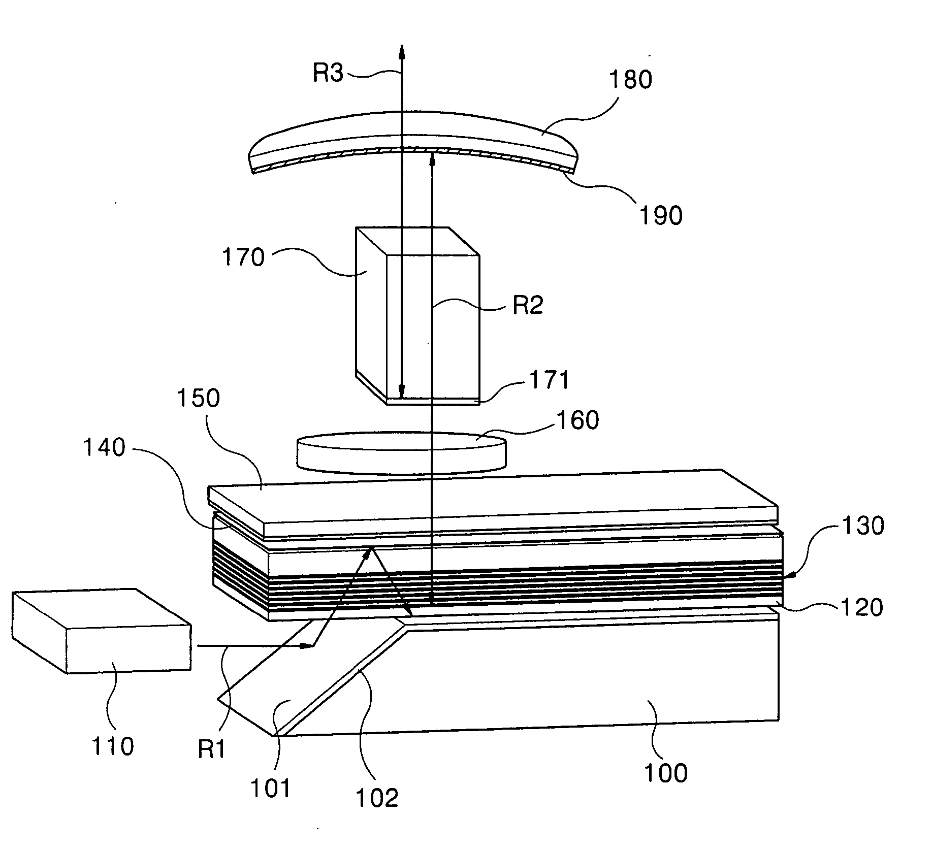
[0046] As shown in FIG. 1, a semiconductor laser includes a substrate 100. The substrate 100 may be formed of silicon carbide (SiC), for example. However, the substrate 100 of another exemplary embodiment may be formed of aluminum nitride (AlN) or gallium arsenide (GaAs).

[0047] A light source 110 is installed outside the substrate 100. Preferably, an applied direction of the light source 110 is substantially perpendicular to a side surface of the substrate 100. The light source 110 may employ a laser diode, which generates a source light referred to as R1, herein. Light R1 emitted from the light source 110 preferably has a wavelength of 808 nm.

[0048] An inclined guide surface 101 is formed at a surface of the substrate 100, to which source light R1 is applied, that reflects the source light R1 in a direction...


PUM


Abstract

An optically pumped semiconductor laser and an optical pumping method are disclosed. The optically pumped semiconductor laser includes first and second reflective bodies forming a resonant region therebetween, a gain medium disposed between the first and second reflective bodies; and a light source for applying a source light to the resonant region in a lateral direction with regard to the gain medium for generating a basic wavelength. The laser further comprising an output mirror and a nonlinear crystal disposed between the output mirror and the second reflective body to generate a predetermined wavelength as a second harmonic of the basic wavelength.

Description

CLAIM OF PRIORITY [0001] This application claims the benefit of the earlier filing date, pursuant to 35 U.S.C. §119, of that patent application filed Jul. 13, 2005 in the Korean Patent Office and afforded Patent Application Serial No. 2005-0063451, the disclosure of which is incorporated by reference in its entirety, herein. BACKGROUND OF THE INVENTION [0002] 1. Field of the Invention [0003] The present invention relates to a semiconductor laser and, more particularly, to an optically pumped semiconductor laser. [0004] 2. Description of Related Art [0005] After the invention of a semiconductor laser, laser technology has been significantly developed with the commercialization of a long-wavelength optical communication laser (1310 nm, 1490 nm, 1550 nm) using an InP substrate and shorter wavelength laser (780 nm, 650 nm) using a GaAs substrate typically used as a CD and DVD pick-up. [0006] In addition, blue-ray disc technology has been developed using a jade green laser (405 nm) on an...

Claims


Application Information

Patent Timeline
Patent Type & Authority Applications(United States)
IPC IPC(8): H01S3/10H01S3/04H01S3/091H01S3/08H01S3/092
CPCB82Y20/00H01S3/094084H01S3/109H01S5/0071H01S5/024H01S2303/00H01S5/141H01S5/18369H01S5/18377H01S5/34306H01S2302/00H01S5/041
Inventor PARK, BYEONG-HOONHWANG, SUN-LYEONGPARK, SUNG-SOO
Owner SAMSUNG ELECTRONICS CO LTD
Why Eureka
Try Eureka