Organic electroluminescence device and method for fabricating the same

a technology of electroluminescent devices and organic el, which is applied in the direction of discharge tubes/lamp details, luminescent screens for discharge tubes, natural mineral layered products, etc., can solve the problems of long service life and efficiency of organic el devices, and achieve the effect of improving service life and efficiency

Active Publication Date: 2007-01-25
LG DISPLAY CO LTD
View PDF24 Cites 57 Cited by
  • Summary
  • Abstract
  • Description
  • Claims
  • Application Information

AI Technical Summary

Benefits of technology

[0009] An object of the present invention is to provide an organic electroluminescent device having an improved service life and efficiency via formation of an electron-transport layer utilizing a novel material, and a method for fabricating the same.
[0010] Another object of the present invention is to provide an organic electroluminescent device involving a simplified manufacturing process via formation of an electron-transport layer utilizing a novel material, and a method for fabricating the same.

Problems solved by technology

Although significant effort has been expended in trying to improve service life and efficiency of conventional organic EL devices, substantially no satisfactory results have been achieved, and service life and efficiency of organic EL devices remain a problem.

Method used


Image

  • Organic electroluminescence device and method for fabricating the same
  • Organic electroluminescence device and method for fabricating the same
  • Organic electroluminescence device and method for fabricating the same

Examples


example 1

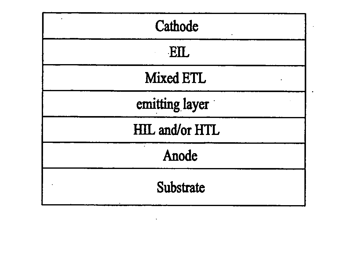
[0071] 1) An anode made of indium tin oxide (ITO) is formed on a transparent substrate, and a hole-injection layer (HIL) made of copper phthalocyanine (CuPc) is applied on the anode to a thickness of about 25 nm.

[0072] 2) A hole transport layer (HTL) is formed by applying 4,4′-bis[N-(1-naphthyl)-N-phenyl-amino]biphenyl (NPD) on the HIL to a thickness of about 35 nm.

[0073] 3) In order to prepare a green-emitting layer, 8-hydroxyquinoline aluminum (Alq3), doped with about 1% C545T, is applied on the HTL to a thickness of about 25 nm.

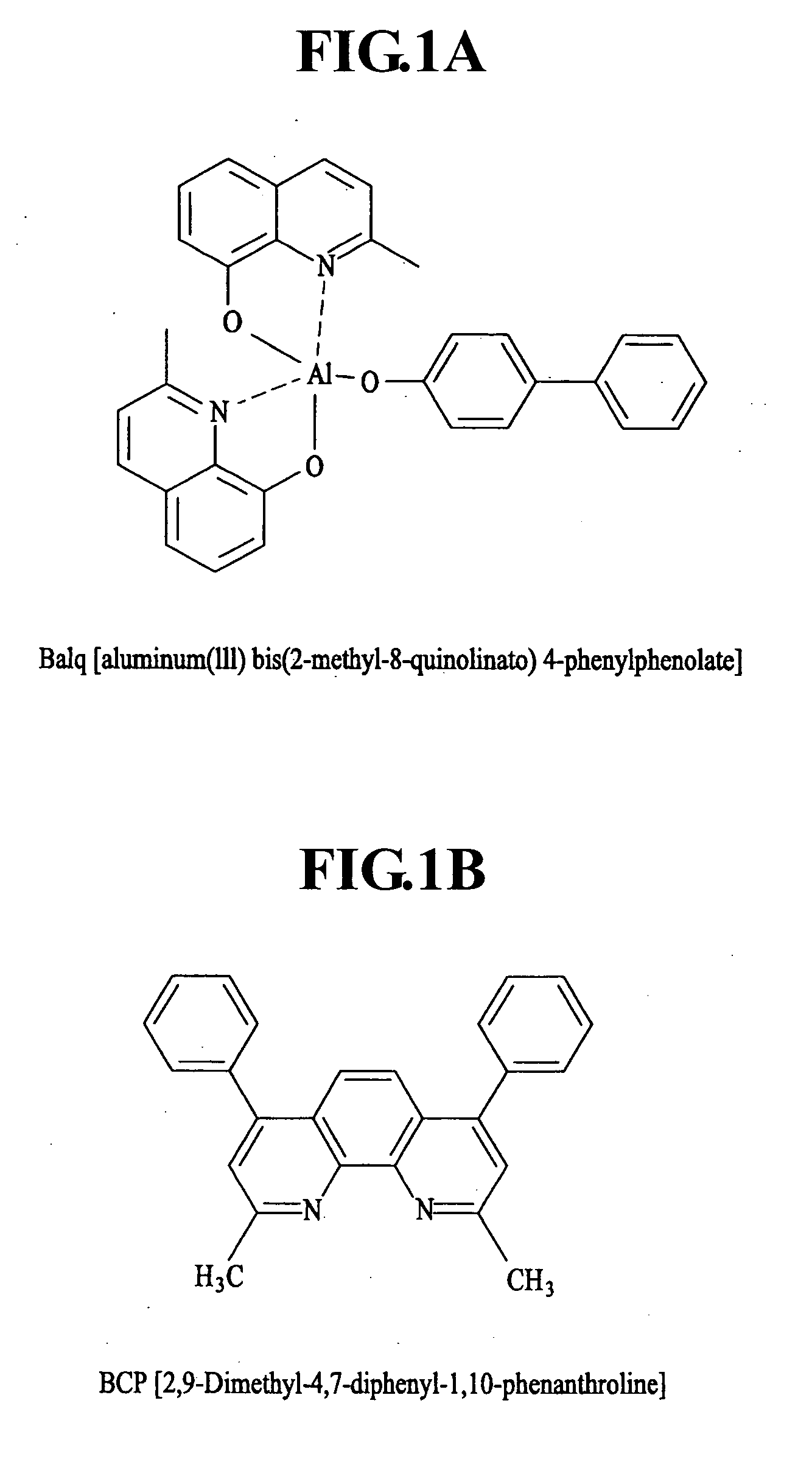
[0074] 4) Alq3 Device A) or Balq (Device B) is applied on the emitting layer to a thickness of about 35 nm to form an electron-transport layer (ETL).

[0075] 5) LiFis applied on the ETL to a thickness of about 0.5 nm to form an electron-injection layer (EIL).

[0076] 6) Aluminum (Al) is applied on the EIL to a thickness of about 150 nm to form a cathode.

[0077] A comparison of IVL characteristics between the Device A and Device B as fabricated in this man...

example 2

[0080]FIG. 10 is a sectional view of an organic EL device in accordance with an embodiment of the invention, and is fabricated as described below.

[0081] 1) An ITO anode is formed on a transparent substrate, and a hole-injection layer (HIL) made of copper phthalocyanine (CuPc) is applied on the anode to a thickness of about 25 nm.

[0082] 2) A hole-transport layer (HTL) is formed by applying 4,4′-bis[N-(1-naphthyl)-N-phenyl-amino]biphenyl (NPD) on the HIL to a thickness of about 35 nm.

[0083] 3) In order to prepare a green-emitting layer, 8-hydroxyquinoline aluminum (Alq3), doped with about 1% C545T, is applied on the HTL to a thickness of about 25 nm.

[0084] 4) An electron-transport layer (ETL) is formed by applying Alq3 having superior electron mobility and Balq having superior hole blocking ability on the emitting layer to a thickness of about 35 nm, in a 3:7 vol % ratio of Balq and Alq3 (Device C), or in a 5:5 vol % ratio of Balq and Alq3 Device D), or in a 7:3 vol % ratio of Bal...

example 3

[0090] Hereinafter, another example of an electron-transport layer which may be utilized in the present invention will be described with respect to FIG. 13.

[0091] The device shown in FIG. 13 was fabricated using BeBq2 as an electron-transporting material and Balq as a hole-blocking material. The electron-transporting capability of BeBq2 is superior to that of Alq3 as used previously, and thus performance of the device could be further enhanced.

[0092] 1) First, an ITO anode is formed on a transparent substrate, and a hole-injection layer (HIL) is formed by applying copper phthalocyanine (CuPc) to a thickness of about 25 nm on the anode.

[0093] 2) A hole-transport layer (HTL) is formed by applying 4,4′-bis[N-(1-naphthyl)-N-phenyl-amino]biphenyl (NPD) to a thickness of about 35 nm on the HIL.

[0094] 3) In order to prepare a green-emitting layer, 8-hydroxyquinoline aluminum (Alq3), doped with about 1% C545T, is applied on the HTL to a thickness of about 25 nm.

[0095] 4) Next, an elect...


PUM

PropertyMeasurementUnit
thicknessaaaaaaaaaa
thicknessaaaaaaaaaa
HOMOaaaaaaaaaa

Abstract

An organic electroluminescent (EL) device is provided which uses an electron-transport layer including hole blocking capability. The device includes a stack structure, with an emitting layer and an electron-transport layer provided between an anode and a cathode. The electron-transport layer is a mixture of at least two materials. This mixture may include an organic compound and one or more other organic compounds, or may include a metal or inorganic compound and one or more other metal or inorganic compounds, or may include one or more organic compounds and one or more metal or inorganic compounds. By incorporating a hole blocking capability into the electron-transport layer, structure and fabrication of the device is simplified and efficiency is increased.

Description

[0001] This application claims the benefit of Korean Patent Application No. 10-2005-0067301, filed on Jul. 25, 2005, which is hereby incorporated by reference as if fully set forth herein. BACKGROUND OF THE INVENTION [0002] 1. Field of the Invention [0003] The present invention relates to an organic electroluminescent (EL) device, and more particularly, to an organic electroluminescent device having an electron-transport layer and a method for fabricating the same. [0004] 2. Background of the Related Art [0005] Generally, an organic electroluminescent (EL) device includes a stack of organic layers, each layer having a function related to an anode made of materials such as indium tin oxide (ITO) and a cathode made of materials such as aluminum (Al). An electric field is applied to the stack to emit light. Organic EL devices are characterized by the capability to be driven at a low voltage with relatively low consumption of electric power, while having a light-weight and flexible subs...

Claims


Application Information

Patent Timeline
Patent Type & Authority Applications(United States)
IPC IPC(8): H01L51/54H01L51/56H05B33/12
CPCH01L27/3211H01L51/005H01L51/0062H01L51/0081H01L51/5072H01L51/5016H01L51/5096H01L51/5278H01L51/0085H10K59/35H10K85/60H10K85/649H10K85/324H10K85/342H10K50/11H10K2101/10H10K50/16H10K50/18H10K50/19C09K11/06H05B33/26
Inventor KIM, MYUNG SEOPSEO, JEONG DAELEE, JAE MANLEE, KYUNG HOONSUNG, CHANG JEPARK, SANG TAECHA, EUN SOO
Owner LG DISPLAY CO LTD
Why Eureka
Try Eureka