

Gas treatment device and heat readiting method
a heat readiting and gas treatment technology, applied in the direction of coatings, chemical vapor deposition coatings, metallic material coating processes, etc., can solve the problems of increasing the number of repeats of film forming operations, difficult to effectively perform temperature control, and affecting the heat dissipation efficiency of the treatment device, so as to prevent the required film forming time from being prolonged, the effect of reducing the thin film forming rate and improving heat dissipation efficiency
- Summary
- Abstract
- Description
- Claims
- Application Information
AI Technical Summary
Benefits of technology
Problems solved by technology
Method used
Image

Examples
first embodiment
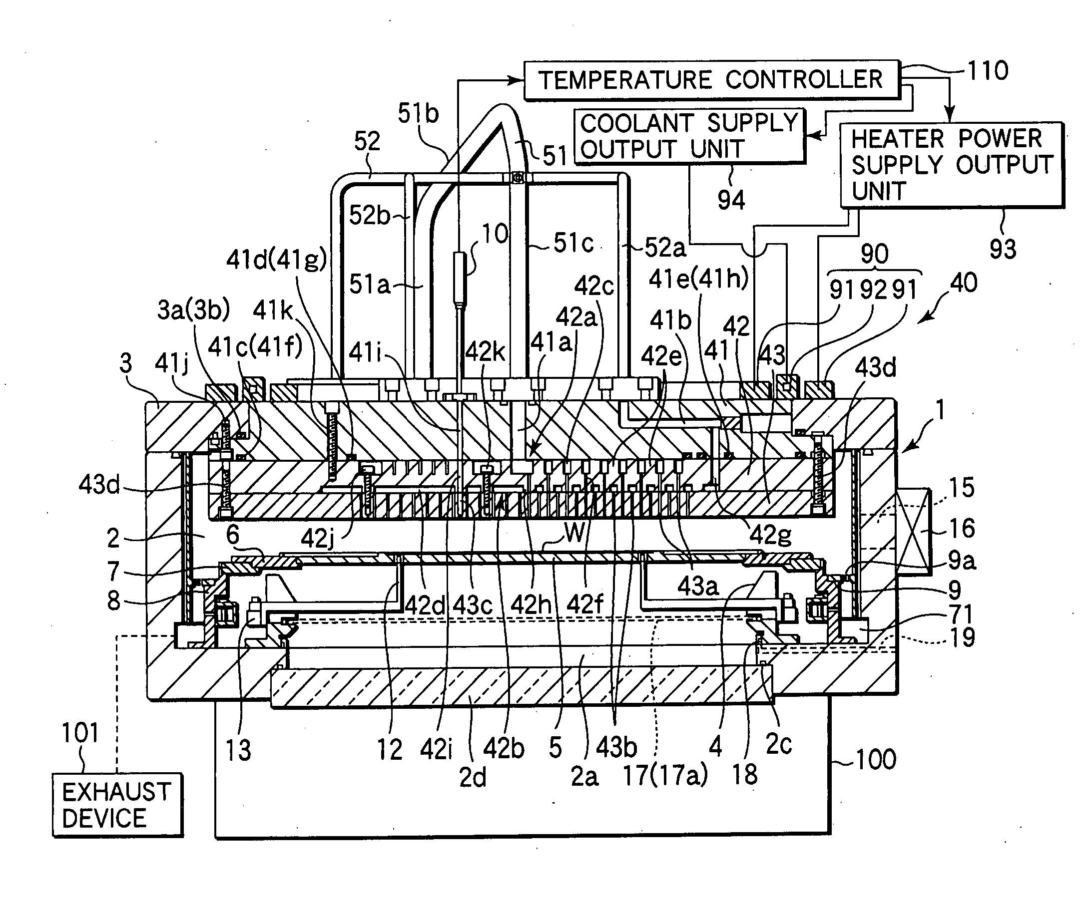
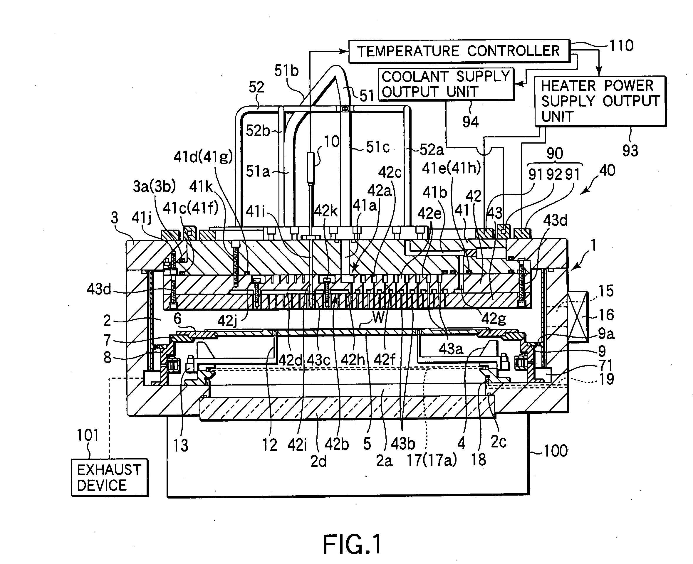
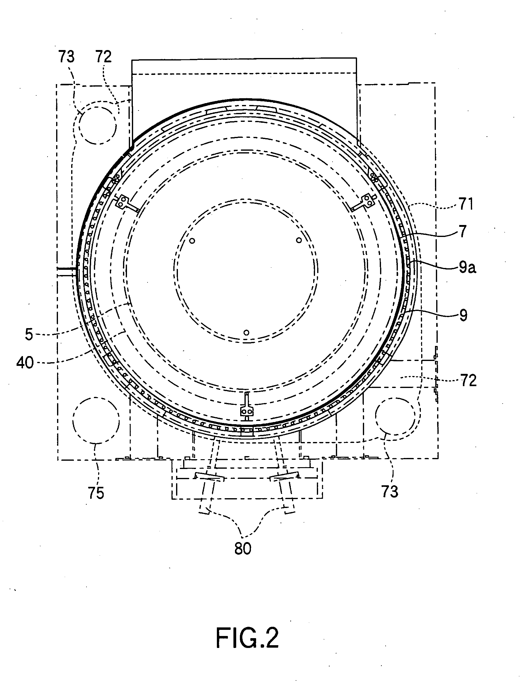
[0059] A first embodiment of the present invention will now be described first. FIG. 1 is a cross sectional view showing the construction of the film-forming apparatus according to a first embodiment of the present invention, FIG. 2 is a plan view showing the inner construction of the housing of the film-forming apparatus according to the first embodiment of the present invention, and FIG. 3 is a plan view showing the upper portion of the housing included in the film-forming apparatus according to the first embodiment of the present invention. Also, FIGS. 4 to 11 show the constituting parts of the shower head included in the film-forming apparatus according to the first embodiment of the present invention.
[0060] Incidentally, FIG. 1 is a cross sectional view of the shower head along the line X-X shown in FIG. 6 referred to herein later. It should be noted that the left portion and the right portion of FIG. 1 relative to the central portion are asymmetric.
[0061] As shown in FIG. 1,...
second embodiment
[0119] A second embodiment of the present invention will now be described.
[0120] In the first embodiment described above, employed is the shower head 40 provided with the heat transfer columns 42e to make it possible to dissipate the heat to the back surface side of the shower head 40 through the heat transfer columns 42e. In addition, the temperature of the shower head 40 can be controlled by the temperature control mechanism 90. However, where a film is formed on the surface (lower surface) of the shower head 40, the heat reflected by the shower head 40 before formation of the film is absorbed by the film formed on the lower surface of the shower head, with the result that it is not able in some cases to suppress sufficiently the temperature elevation with time of the shower head 40 by relying on the heat transfer columns 42e and the temperature control mechanism 90 alone. It follows that a nonuniformity of the film quality and the film composition is caused among the wafers.
[01...
third embodiment
[0128] A third embodiment of the present invention will now be described.
[0129] In order to realize the temperature control of the shower head with a high precision as in the example of the construction shown in FIGS. 22 and 23, it is desirable to arrange a heating means and a cooling means in a manner to permit the heating and the cooling to be performed over a large range on the upper surface of the shower head 40. In view of the particular situation, a temperature control mechanism 130 is formed by alternately arranging annular heaters 131a, 131b, 131c and annular coolant passages 132a, 132b and 132c on the upper surface of the shower head 40 as shown in FIG. 25, thereby making it possible to heat and cool substantially the entire region of the upper surface of the shower head 40. The power supply to these heaters 131a, 131b and 131c and the temperature and the flow rate of coolant circulated in the coolant passages 132a, 132b and 132c are controlled based on the detection signa...
PUM
| Property | Measurement | Unit |
|---|---|---|
| Diameter | aaaaa | aaaaa |
| Temperature | aaaaa | aaaaa |
| Thickness | aaaaa | aaaaa |
Abstract
Description
Claims
Application Information