Compositionally-graded photovoltaic device and fabrication method, and related articles

Inactive Publication Date: 2007-02-01
GENERAL ELECTRIC CO
View PDF14 Cites 100 Cited by
  • Summary
  • Abstract
  • Description
  • Claims
  • Application Information

AI Technical Summary

Problems solved by technology

Moreover, polycrystalline semiconductor materials may contain randomly-oriented grains, with grain boundaries which induce a large number of bulk and surface defect states.
The presence of various defects of this type can be the source of deleterious effects in the photovoltaic device.
Thus, they become lost as current carriers.
This new interface is yet another site for impurities and spurious contaminants to become trapped and to accumulate, a

Method used


Image

  • Compositionally-graded photovoltaic device and fabrication method, and related articles
  • Compositionally-graded photovoltaic device and fabrication method, and related articles
  • Compositionally-graded photovoltaic device and fabrication method, and related articles

Examples


example 1

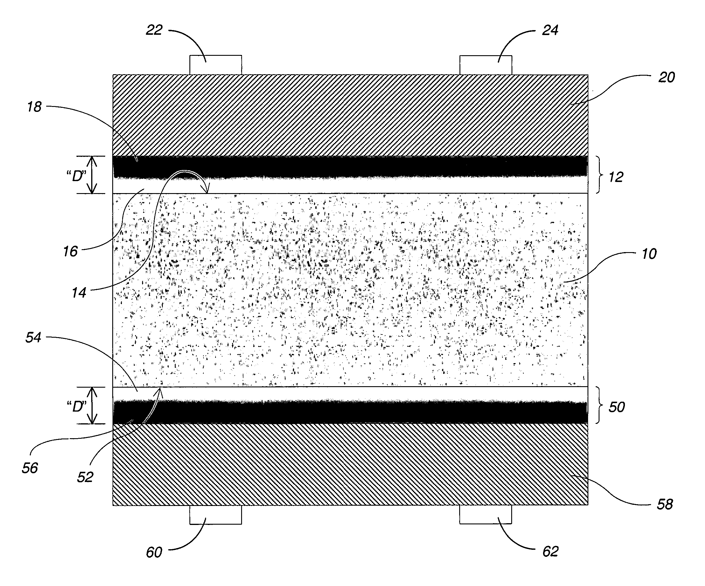
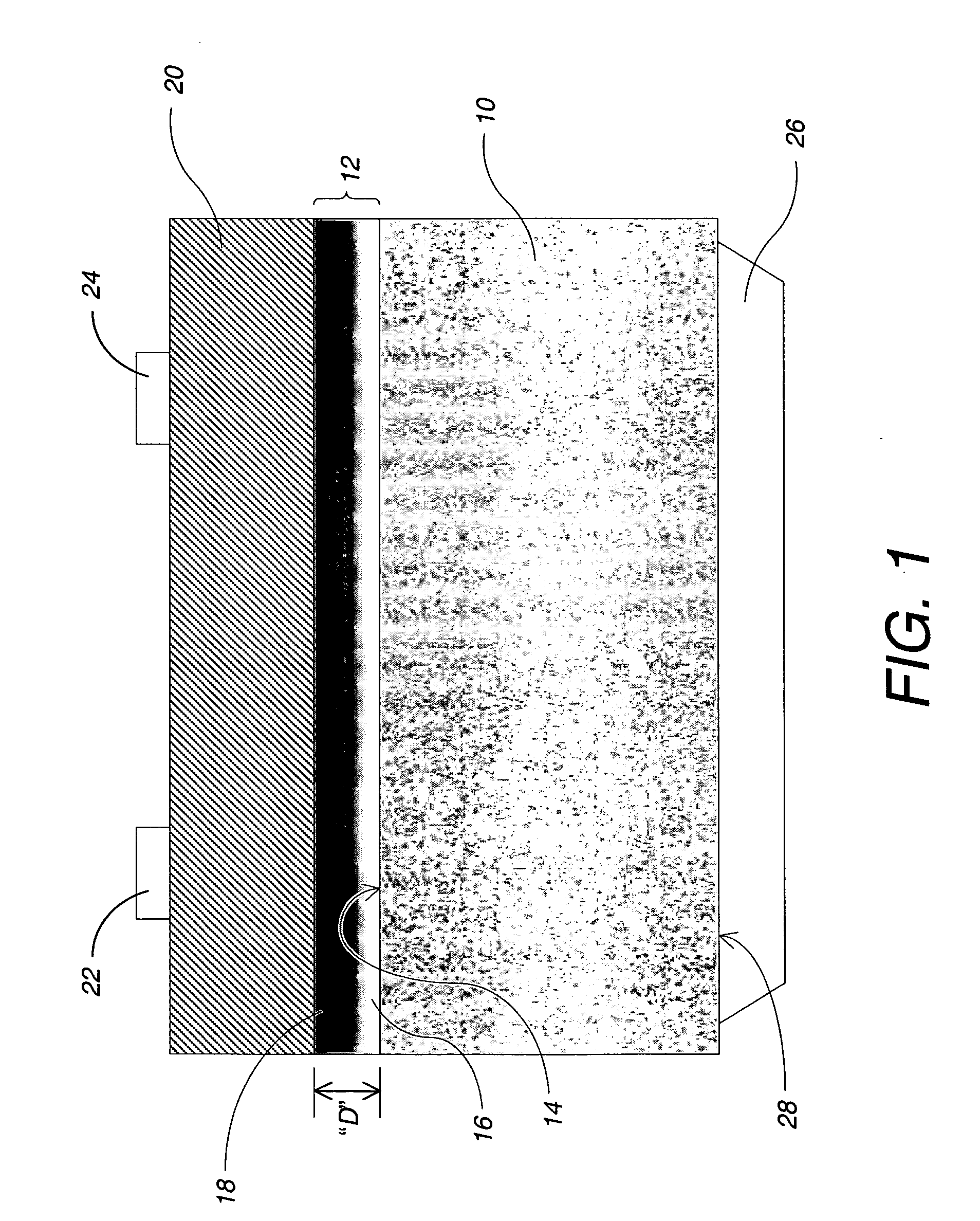
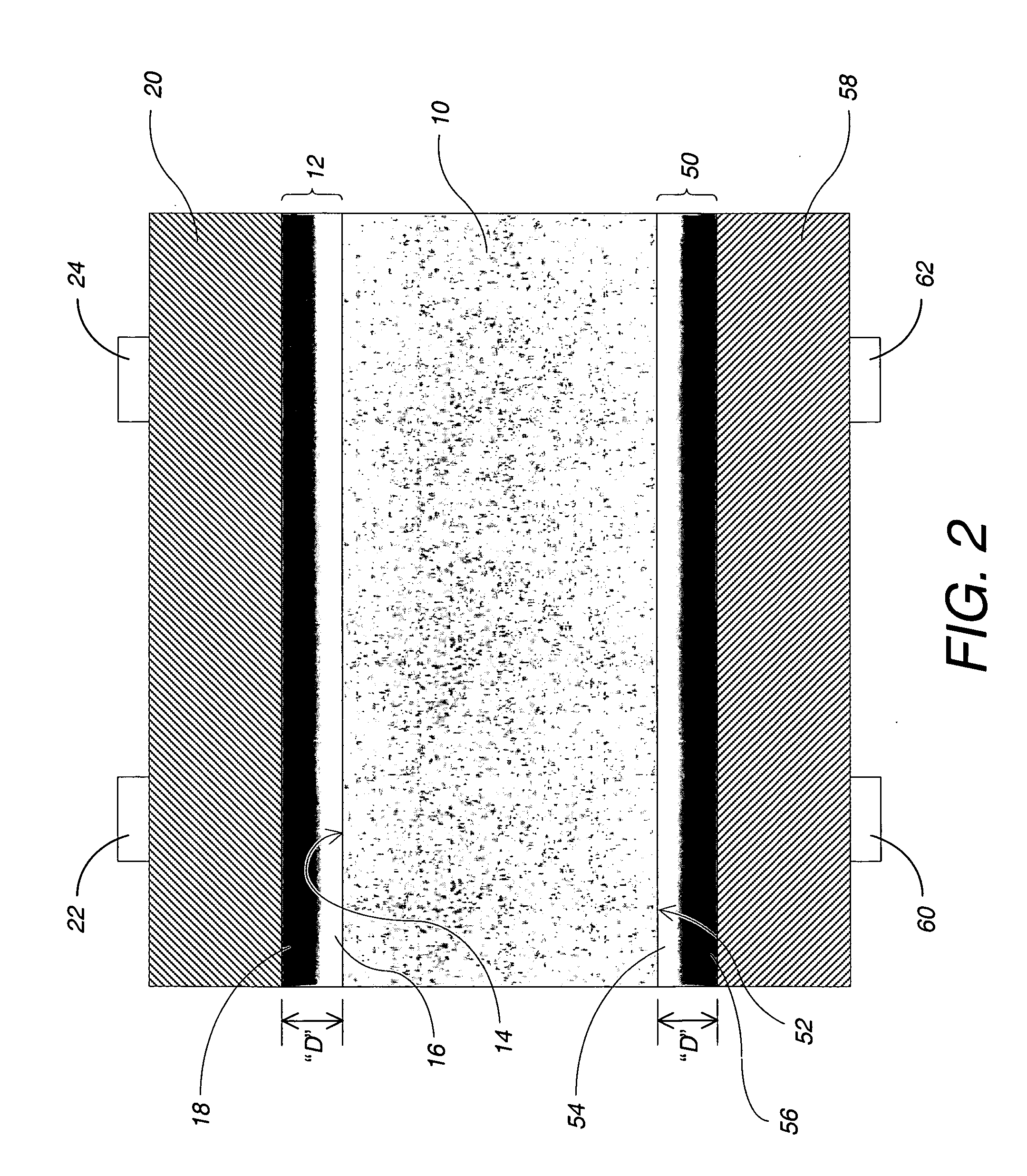
[0047] This example provides a non-limiting illustration of the fabrication of photovoltaic devices according to some embodiments of the present invention. Monocrystalline or polycrystalline semiconductor substrates of one conductivity type are placed in a plasma reaction chamber (for example: a plasma enhanced chemical vapor deposition system). A vacuum pump removes atmospheric gases from the chamber. The substrates to be processed are preheated to about 120 to about 24° C. A hydrogen plasma surface preparation step is performed prior to the deposition of the compositionally graded layer. Hydrogen (H2) is introduced into the chamber at a flow rate of about 50 to about 500 sccm (standard cubic centimeters per minute). A throttle valve is used to maintain a constant processing pressure in the range of about 200 mTorr to about 800 mTorr. Alternating frequency input power with a power density in the range of about 6 mW / cm2 to about 50 mW / cm2 range is used to ignite and maintain the pla...


PUM


Abstract

A semiconductor structure is described, including a semiconductor substrate of one conductivity type; and an amorphous semiconductor layer disposed on at least one of its surfaces. The amorphous semiconductor layer is compositionally graded through its depth, from substantially intrinsic at the interface with the substrate, to substantially conductive at the opposite side. Photovoltaic devices which include such a structure are also disclosed, as are solar modules made from one or more of the devices. Related methods are also described.

Description

[0001] This patent application claims the benefit of pending provisional application Ser. No. 60 / 704,181 (Attorney Dkt. 188359-1), filed on Jul. 28, 2005.BACKGROUND OF THE INVENTION [0002] This invention relates generally to the field of semiconductor devices which include a heterojunction, such as a photovoltaic device. [0003] Devices which rely on the presence of a heterojunction are well-known in the art. (As used in this context, a heterojunction is usually formed by contact between a layer or region of one conductivity type with a layer or region of opposite conductivity, e.g., a “p-n” junction). Examples of these devices include thin film transistors, bipolar transistors, and photovoltaic devices (e.g., solar cells). [0004] Photovoltaic devices convert radiation, such as solar, incandescent, or fluorescent radiation, into electrical energy. Sunlight is the typical source of radiation for most devices. The conversion to electrical energy is achieved by the well-known photovolta...

Claims


Application Information

Patent Timeline
IPC IPC(8): H01L31/00H02N6/00H01L31/065H01L31/072H01L31/075
CPCH01L31/065H01L31/072Y02E10/548H01L31/075H01L31/202H01L31/0747Y02P70/50
Inventor JOHNSON, JAMES NEILMANIVANNAN, VENKATESAN
Owner GENERAL ELECTRIC CO
Why Eureka
Try Eureka