This helps you quickly interpret patents by identifying the three key elements:
Problems solved by technology
Method used
Benefits of technology
Benefits of technology
[0012] An object of the present invention is therefore to provide an electron beam detection device that is capable of preventing response speed from being decreased and reducing noise to thereby detect electrons with good response and high sensitivity and an electron tube that uses the electron beam detection apparatus. Arrangement Solving the Problem
[0039] According to the electron tube having the above configuration, the electro-optic converter is disposed near the semiconductor device. Therefore, the response of signals is prevented from being impaired. Electrical signals can be converted into optical signals without being deteriorated and supplied to an external circuit.
Problems solved by technology
Therefore, separate installation of the semiconductor device and signalprocessing circuit is unfavorable, in terms of response speed and in terms of signal quality which may be deteriorated due to noise.
Method used
Image
Click on the blue label to locate the original text in one second.
Reading with bidirectional positioning of images and text.
Examples
first modification
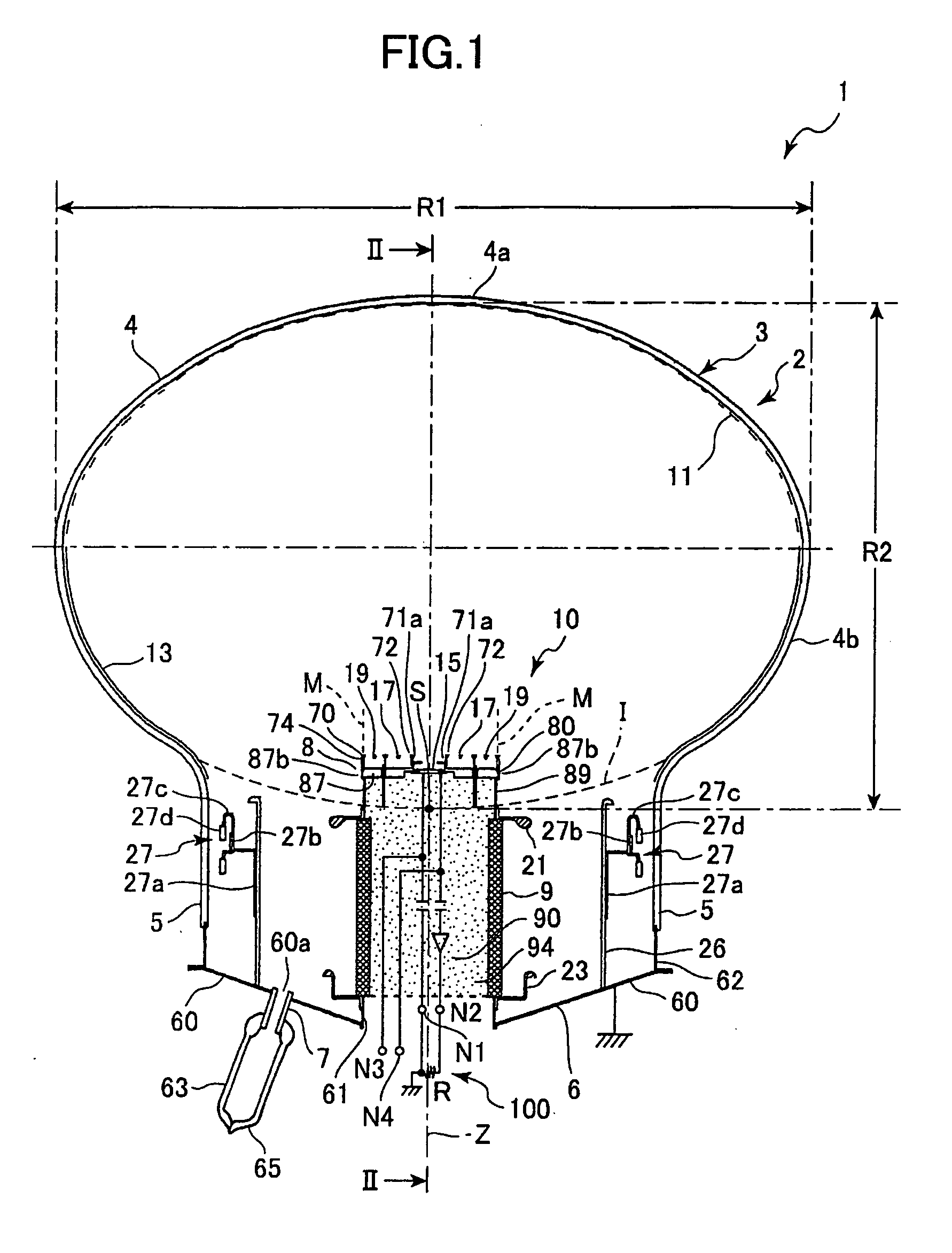
[0200] As shown in FIG. 13, the vertical cross-section of the glass bulb body 4 including the axis Z may be substantially a circular shape. In this case, the diameter of the glass bulb body 4 perpendicular to the axis Z is substantially equal to the diameter thereof parallel to the axis Z.
[0201] Also in this case, the APD 15 may be disposed on the glass bulb body 4 side (upper side in FIG. 13) relative to the reference point S at which the imaginary extended curved surface I of the lower hemisphere 4b of the glass bulb body 4 crosses the axis Z in the glass bulb base 5. The point c denotes the center of the glass bulb body 4.
[0202] Equipotential surfaces E are generated by a potential difference between the envelope 2 and the APD 15 and, accordingly, the electrons from the photocathode 11 fly along the trajectories L. Therefore, the electrons are converged on a point P3 in the vicinity of the upper surface of the APD 15, which is located slightly below the point C.
[0203] By dispo...
second modification
[0205] In the above embodiment, the leading end 21c of the conductive flange 21 has a rounded shape having a greater thickness than that of the flange body 21b. Alternatively, however, the configuration of the leading end 21c of the conductive flange 21 may be obtained by rolling up the outer periphery of the flange body 21b, as shown in FIG. 15.
[0206] Similarly, the configuration of the leading end 23d of the conductive flange 23 may be obtained by rolling up the outer periphery 23d of the rising portion 23c.
third modification
[0207] As described with reference to FIG. 3, in the above embodiment, the cap 73 of the shield portion 70 has the inner wall 72, ceiling 76, and outer wall 74. Alternatively, however, the inner wall 72 and ceiling 76 may be removed from the cap 73, as shown in FIG. 16. In this case, the cap 73 is constituted by only the outer wall 74.
[0208] Also in this case, the manganese beads 17 and antimony beads 19 are disposed at the portions on the upper side (i.e., the upper hemisphere 4a side) relative to the base 87 and between outer wall 71a of the cover 71 and imaginary extended curved surface M of the outer periphery 87b of the base 87, as in the above embodiment which has been described with reference to FIG. 1. Therefore, the base 87 and outer wall 74 prevents the manganese vapor or antimony vapor from being adhered to the internal surface of the glass bulb base 5, the outer stem 6, or lower hemisphere 4b. Further, the cover 71 prevents the manganese vapor or antimony vapor from bei...
PUM
Abstract
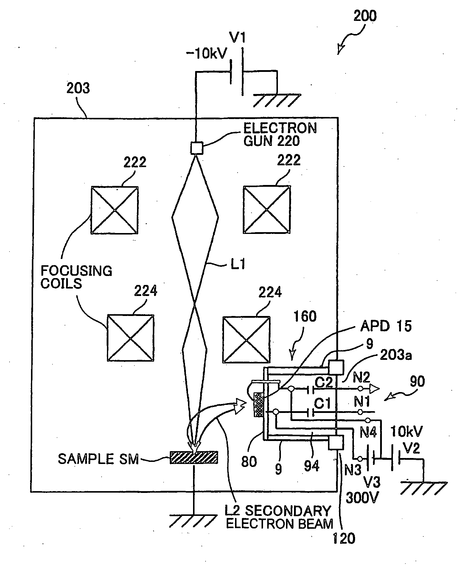
An insulating tube has one end and another end. An An avalanche photodiode (APD) is provided outside the one end of the insulating tube. The another end of the insulating tube is air-tightly connected to an outer flange through a stem inner wall. Capacitors electrically connected to the APD are provided in the insulating tube. The capacitors remove direct current components from signals that the APD generates when detecting electrons. By providing the capacitors in the insulating tube, response of output signals can be prevented from being impaired.
Description
TECHNICAL FIELD [0001] The present invention relates to an electron beam detection device and an electron tube. BACKGROUND ART [0002] Various electron tubes have been proposed. The electron tube have a photocathode that emits photoelectrons in response to an incident light and an electron-bombarded semiconductor device, such as an avalanche photodiode (hereinafter, referred to as APD) that amplifies the photoelectrons so as to detect them. [0003] As an electron tube using the APD, there has been proposed an electron tube having an entrance window inside of which a photocathode is formed and a conductive stem on which the APD is disposed. The entrance window is provided at the opening of an insulating container, and the conductive stem is provided opposed to the photocathode of the insulating container. A signal output from the APD is input to an electrical circuit provided outside the insulating container through a lead pin and thereby the incident electrons are detected. The electr...
Claims
Application Information
Patent Timeline
Application Date:The date an application was filed.
Publication Date:The date a patent or application was officially published.
First Publication Date:The earliest publication date of a patent with the same application number.
Issue Date:Publication date of the patent grant document.
PCT Entry Date:The Entry date of PCT National Phase.
Estimated Expiry Date:The statutory expiry date of a patent right according to the Patent Law, and it is the longest term of protection that the patent right can achieve without the termination of the patent right due to other reasons(Term extension factor has been taken into account ).
Invalid Date:Actual expiry date is based on effective date or publication date of legal transaction data of invalid patent.

