Semiconductor device and method of fabricating the same

a semiconductor device and semiconductor technology, applied in the direction of semiconductor devices, electrical devices, transistors, etc., can solve the problems of more likely to occur current leakage, current leakage may occur, and conventional semiconductor devices have failed to suppress current leakage at the contact, etc., to achieve shorten the distance between the gate and the gate, suppress current leakage, and micronize the effect of semiconductor devices

Active Publication Date: 2007-02-01
RENESAS ELECTRONICS CORP
View PDF10 Cites 31 Cited by
  • Summary
  • Abstract
  • Description
  • Claims
  • Application Information

AI Technical Summary

Benefits of technology

[0034] According to the present invention, even in a configuration having, in a partial region thereof, the sidewall on the side face of the gate electrode and having the source / drain extension region (or LDD: lightly doped drain) formed therebelow in a self-aligned manner, the region having the shared contact formed therein can be configured as having no source / drain extension region formed beside the gate electrode. The shared contact is no more in contact with the region having a low impurity concentration in the surficial portion of the semiconductor substrate, even if the side wall has been removed in the process of forming the contact which allows therein electrical connection of the gate electrode and the impurity-diffused region connected through the shared contact. For this reason, it is made possible to suppress the current leakage at the shared contact connecting the gate electrode and the impurity-diffused region.
[0035] In general, the impurity-diffused region such as source / drain extension region of MOS transistors is formed by implanting ion over the entire surface. Therefore the semiconductor region located beside the gate electrode of the MOS transistor containing the source / drain extension region will have the source / drain extension region having a predetermined width. In the shared contact structure connecting the gate electrode and the impurity-diffused region, micronization can be realized by shortening the distance between the gate and the impurity-diffused region. However for the case where a portion of the gate electrode, used also as the gate electrode of a MOS transistor, is used as a connection point with the shared contact, excessively shortened distance between the gate electrode and the semiconductor region will undesirably result in formation of the source / drain extension region beside the gate electrode also at the connection point with the shared contact. In this case, removal-by-etching of the sidewall in the process of formation of the contact hole will cause the problem of current leakage as described in the above. The semiconductor device and the method of fabricating the same according to the present invention are configured so as to make the distance between the gate electrode and impurity-diffused region substantially equal to the width of the sidewall, and so as to form the element-isolating insulating film under the contact in the region between the gate electrode and the impurity-diffused region. It is therefore made possible to avoid the problem of current leakage, and to realize micronization of the semiconductor device.
[0036] According to the present invention, there is provided a technique of micronizing the semiconductor device, and of suppressing current leakage at the shared contact connecting the gate electrode and the impurity-diffused region.

Problems solved by technology

For this reason, a problem has been arisen in that current leakage may occur in a region where the shared contact 12 comes into contact with the source / drain extension region 69a.
In particular, such current leakage is more likely to occur when the source / drain extension region is formed only to a small depth.
The conventional semiconductor device has, however, failed in suppressing the current leakage at the contact interconnecting the gate electrode and the impurity-diffused region as the micronization advances.
However, as shown in FIG. 7 in the literature by F. Arnaud et al., a problem arose in that the STI in a shared contact forming region was considerably removed, and another current leakage would occur.

Method used


Image

  • Semiconductor device and method of fabricating the same
  • Semiconductor device and method of fabricating the same
  • Semiconductor device and method of fabricating the same

Examples


Embodiment Construction

[0048] The invention will be now described herein with reference to an illustrative embodiment. Those skilled in the art will recognize that many alternative embodiments can be accomplished using the teachings of the present invention and that the invention is not limited to the embodiment illustrated for explanatory purposes.

[0049] Paragraphs below will explain an embodiment of the present invention, referring to the attached drawings. It is to be noted that, in all drawings, any constituents commonly appear will be given with the same reference numerals, so as to appropriately omit the explanation.

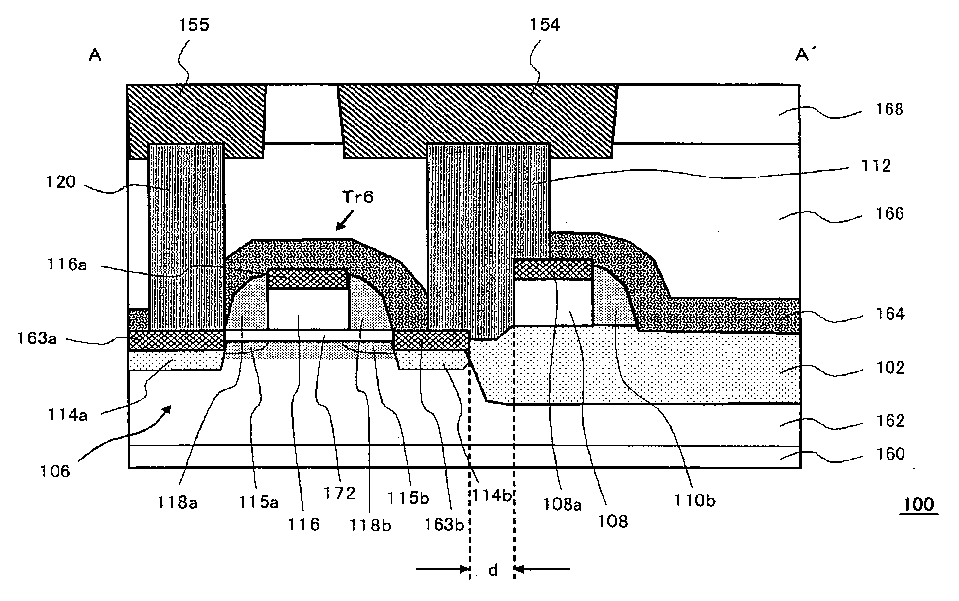
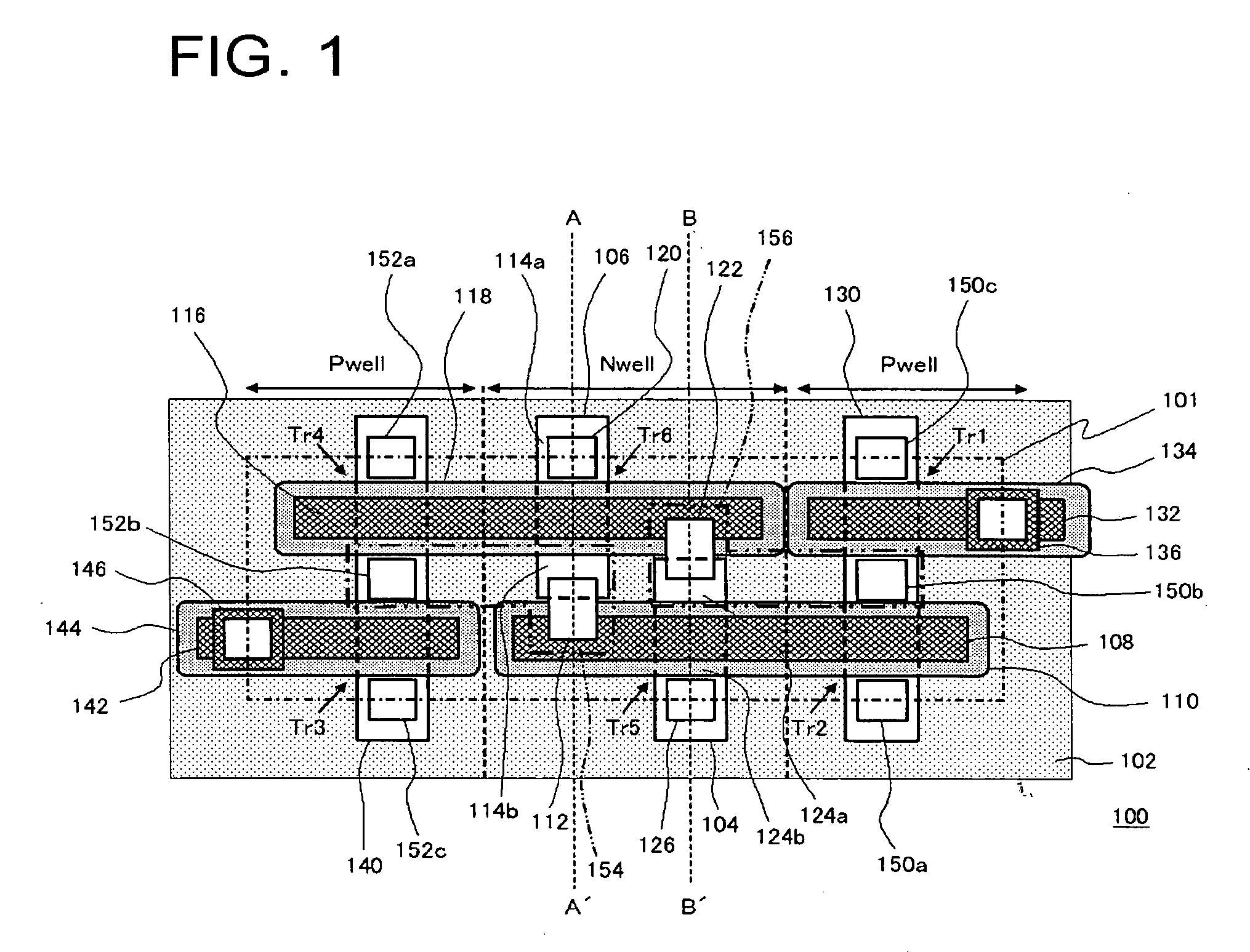
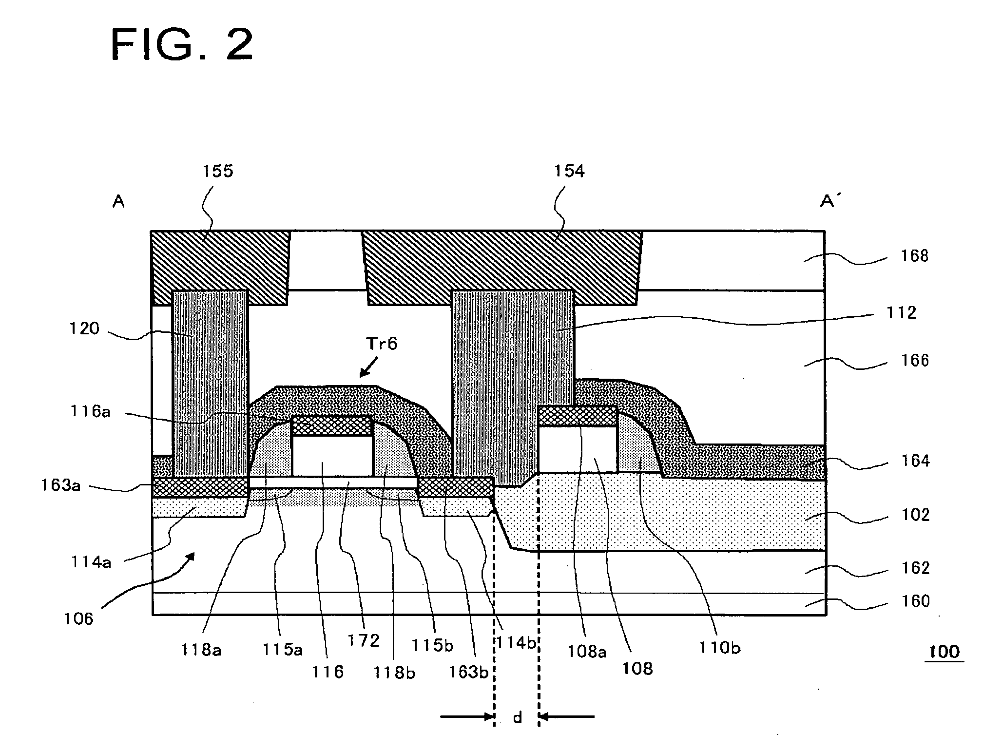
[0050]FIGS. 8A and 8B are schematic drawings explaining a configuration of a semiconductor device 100 according to the embodiment of the present invention. FIG. 8A is a schematic top view of the semiconductor substrate, and FIG. 8B is a schematic top view shown in FIG. 8A, overlaid with a sectional structure taken along a first section and a second section.

[0051] As shown in FIGS. 8A ...


PUM


Abstract

In view of micronizing semiconductor device and of suppressing current leakage in a shared contact allowing contact between a gate electrode and an impurity-diffused region, a semiconductor device 100 includes a first gate electrode 108, a fourth source/drain region 114b, and a shared contact electrically connecting the both, wherein in a section taken along the gate length direction, the first gate electrode 108 and the fourth source/drain region 114b are disposed as being apart from each other, an element-isolating insulating film 102 is formed over the entire surface of a semiconductor substrate 160 exposed therebetween, and the distance between the first gate electrode 108 and the fourth source/drain region 114b is made substantially equal to the width of the sidewall formed on the side face of the first gate electrode 108, when viewed in another section taken along the gate length direction.

Description

[0001] This application is based on Japanese patent applications No. 2005-222493 and No. 2006-159567 the contents of which are incorporated hereinto by reference. DISCLOSURE OF THE INVENTION TECHNICAL FIELD [0002] The present invention relates to a semiconductor device containing a shared contact connecting a gate electrode and a impurity-diffused region, and a method of fabricating the same. RELATED ART [0003] Inverter circuit, for example, uses an interconnection structure electrically connecting a gate electrode of a MOS (metal-oxide-semiconductor) field effect transistor (referred to as “MOS transistor”, hereinafter) and an impurity-diffused region such as source / drain region. [0004] Japanese Laid-Open Patent Publication No. H7-115198 discloses a local interconnection structure connecting a gate electrode formed on a field oxide film and a source / drain region. Japanese Laid-Open Patent Publication No. S61-168265 and Japanese Laid-Open Patent Publication No. 2002-270701 disclose ...

Claims


Application Information

Patent Timeline
Patent Type & Authority Applications(United States)
IPC IPC(8): H01L29/76
CPCH01L21/76895H01L21/76897H01L27/11H01L29/7833H01L29/665H01L29/6653H01L29/6659H01L27/1104H10B10/00H10B10/12
Inventor MATSUI, KOUJIROU
Owner RENESAS ELECTRONICS CORP
Why Eureka
Try Eureka