

Piezoelectric thin film element
a thin film, piezoelectric technology, applied in the direction of piezoelectric/electrostriction/magnetostriction machines, device material selection, generators/motors, etc., can solve the problems of noticeable property variation and degradation, sintered piezoelectric substances or piezoelectric thin films comprising above-mentioned pzt, undesirable effects of thickness, etc., to achieve excellent dielectric strength voltage
- Summary
- Abstract
- Description
- Claims
- Application Information
AI Technical Summary
Benefits of technology
Problems solved by technology
Method used
Image

Examples
first embodiment
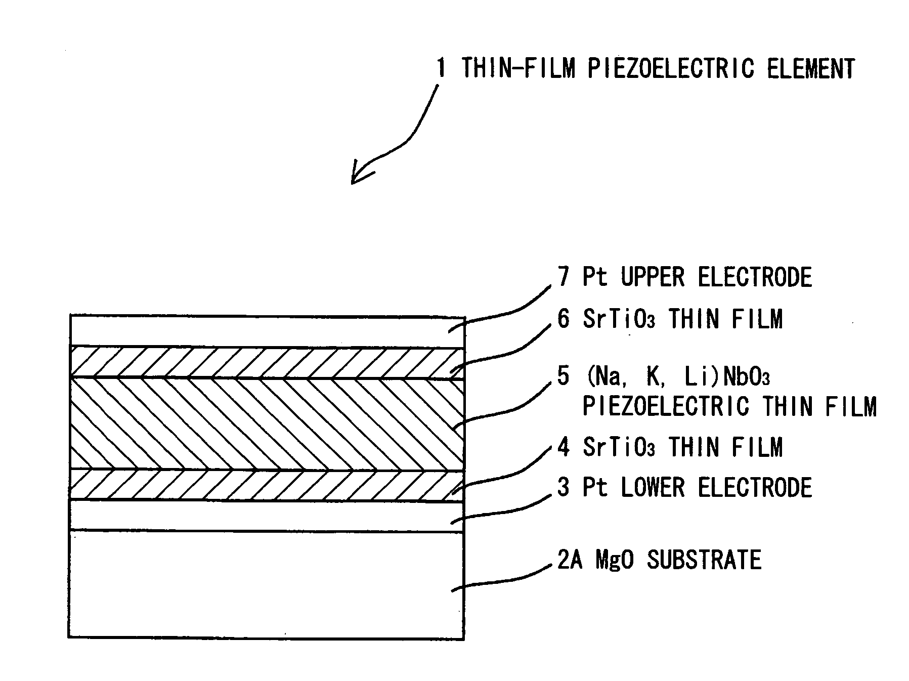
[0048]FIG. 1 illustrates a thin-film piezoelectric element according to a first preferred embodiment of the invention. A thin-film piezoelectric element 1 according to the first embodiment includes a MgO substrate 2A consisting of a MgO single crystal. Using RF (high-frequency) magnetron sputtering, on this MgO substrate 2A, there are sequentially formed a Pt lower electrode 3, a first SrTiO3 thin film 4 as a high voltage-withstand dielectric, a piezoelectric thin film 5, a second SrTiO3 thin film 6 as a high voltage-withstand dielectric, and a Pt upper electrode 7. The first SrTiO3 thin film 4, piezoelectric thin film 5, and second SrTiO3 thin film 6 make up a piezoelectric portion.
[0049] The piezoelectric thin film 5 is made of a dielectric thin film expressed by general formula (NaxKyLiz)NbO3 (03 piezoelectric thin film 5.
[0050] The SrTiO3 thin films 4 and 6 have a 1 MV / cm or higher dielectric strength voltage, which is greater than that of the (Na, K, Li)NbO3 piezoelectric thi...
second embodiment
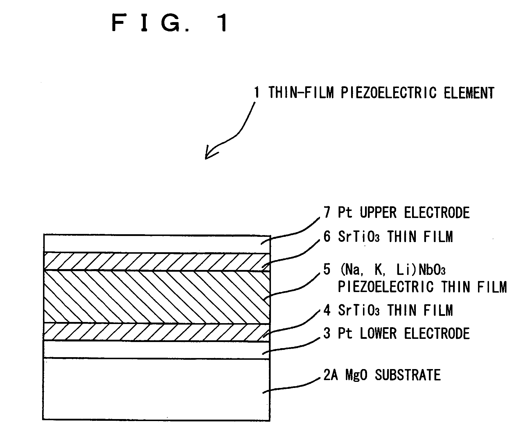
[0057]FIG. 2 illustrates a thin-film piezoelectric element according to a second preferred embodiment of the present invention. A thin-film piezoelectric element 1 according to the second embodiment includes a SrTiO3 thin film 4 formed only underneath a (Na, K, Li)NbO3 piezoelectric thin film 5. Specifically, in this embodiment, using RF (high-frequency) magnetron sputtering, on a MgO substrate 2A consisting of a MgO single crystal, there are sequentially formed a Pt lower electrode 3, a SrTiO3 thin film 4, a (Na, K, Li)NbO3 piezoelectric thin film 5, and a Pt upper electrode 7. The SrTiO3 thin film 4 and piezoelectric thin film 5 make up a piezoelectric portion.
[0058] This second embodiment can offer the following advantages: [0059] (a) Stacking to the (Na, K, Li)NbO3 piezoelectric thin film 5 the SrTiO3 thin film 4 having excellent dielectric strength voltage allows enhancement in voltage withstand of the entire piezoelectric portion comprising the SrTiO3 thin film 4 and the (Na,...
third embodiment
[0062]FIG. 3 illustrates a thin-film piezoelectric element according to a third preferred embodiment of the present invention. A thin-film piezoelectric element 1 according to the third embodiment includes a SrTiO3 thin film 6 formed only on a (Na, K, Li)NbO3 piezoelectric thin film 5. Specifically, in this embodiment, using RF magnetron sputtering, on a MgO substrate 2A consisting of a MgO single crystal, there are sequentially formed a Pt lower electrode 3, a (Na, K, Li)NbO3 piezoelectric thin film 5, a SrTiO3 thin film 6, and a Pt upper electrode 7. The (Na, K, Li)NbO3 piezoelectric thin film 5 and SrTiO3 thin film 6 make up a piezoelectric portion.
[0063] This third embodiment can offer the following advantages: [0064] (a) Stacking to the (Na, K, Li)NbO3 piezoelectric thin film 5 the SrTiO3 thin film 6 having excellent dielectric strength voltage allows enhancement in voltage withstand of the entire piezoelectric portion comprising the (Na, K, Li)NbO3 piezoelectric thin film 5 a...
PUM
| Property | Measurement | Unit |
|---|---|---|
| Width | aaaaa | aaaaa |
| Dielectric strength | aaaaa | aaaaa |
| Electric potential / voltage | aaaaa | aaaaa |
Abstract
Description
Claims
Application Information