Methodology for layout-based modulation and optimization of nitride liner stress effect in compact models

a technology of nitride liner and compact model, applied in the direction of cad circuit design, program control, instruments, etc., can solve the problems of reducing the stress benefit, affecting the ability of long film runway, and difficult to predict the effect of performance, either positive or negativ

Active Publication Date: 2007-02-01
GLOBALFOUNDRIES US INC
View PDF6 Cites 67 Cited by
  • Summary
  • Abstract
  • Description
  • Claims
  • Application Information

AI Technical Summary

Benefits of technology

[0009] The present invention provides a system and method that address the above and other issues by providing a computationally efficient technique that accurately accounts for layout-induced changes caused by nitride liner-based stress in semiconductor devices. In particular, the invention uses methods and algorithms to account for the impact of differences in circuit layout style on circuit performance. Such algorithms are implemented for obtaining the appropriate stress functional approximations and in extraction algorithms to obtain the correct geometric parameters.

Problems solved by technology

One factor that dilutes the effectiveness of nitride liners is that the contact metallurgy, particularly to the source and drain regions, requires parts of the liner to be etched away very near the device.
This not only disrupts the ability of the long film runway to transfer stress, but also moves the singularity / edge that would influence the channel further away, severely reducing the stress benefit.
Further, an even more serious concern is that these structures can be arbitrarily designed and therefore have a difficult to predict effect on performance, either positive or negative.
Not accounting for this magnitude of variation in stress benefit can seriously underpredict or overpredict electrical performance in circuit simulation.
This impact causes circuit operability problems and therefore must be properly accounted for.

Method used


Image

  • Methodology for layout-based modulation and optimization of nitride liner stress effect in compact models
  • Methodology for layout-based modulation and optimization of nitride liner stress effect in compact models
  • Methodology for layout-based modulation and optimization of nitride liner stress effect in compact models

Examples


Embodiment Construction

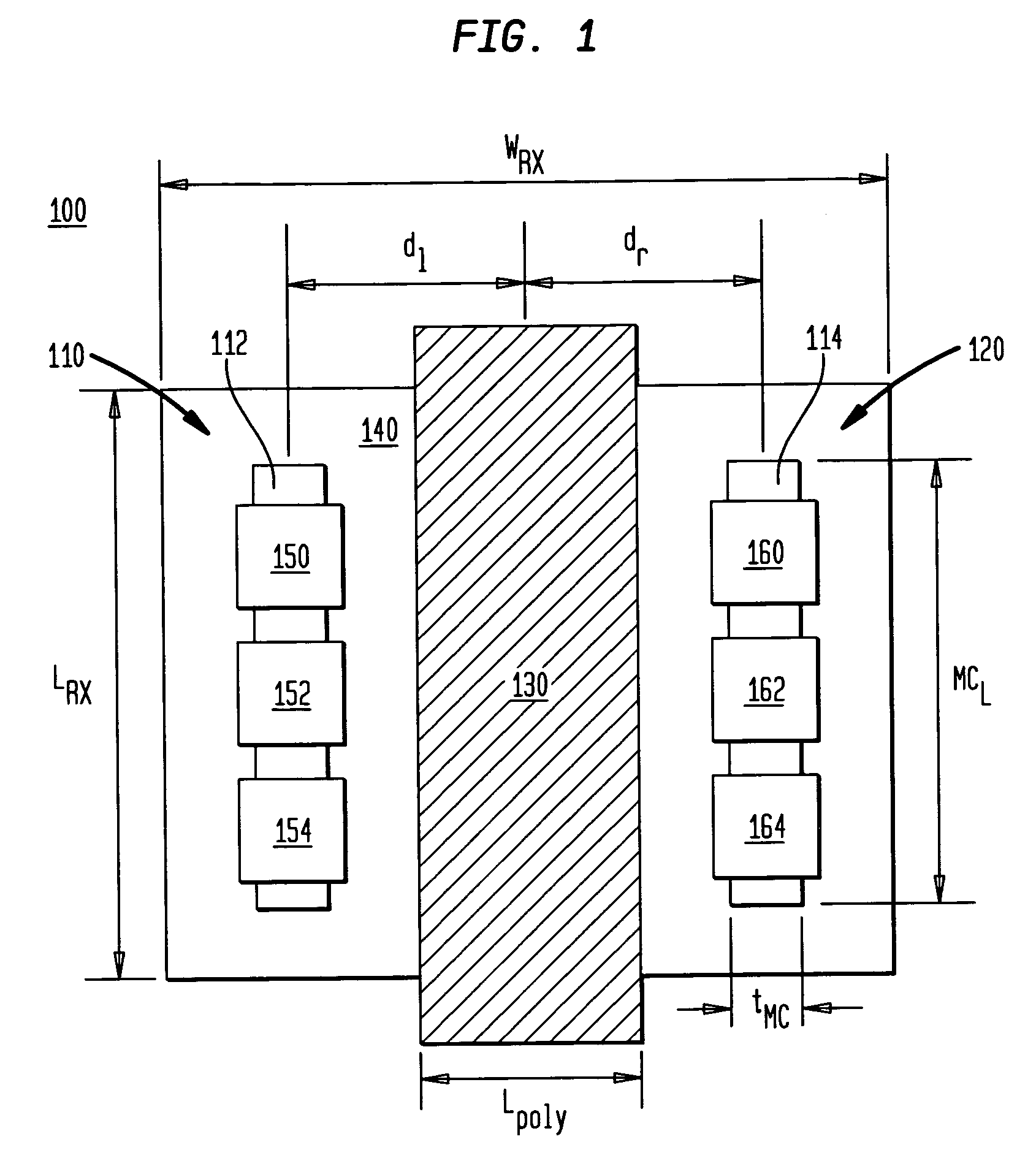
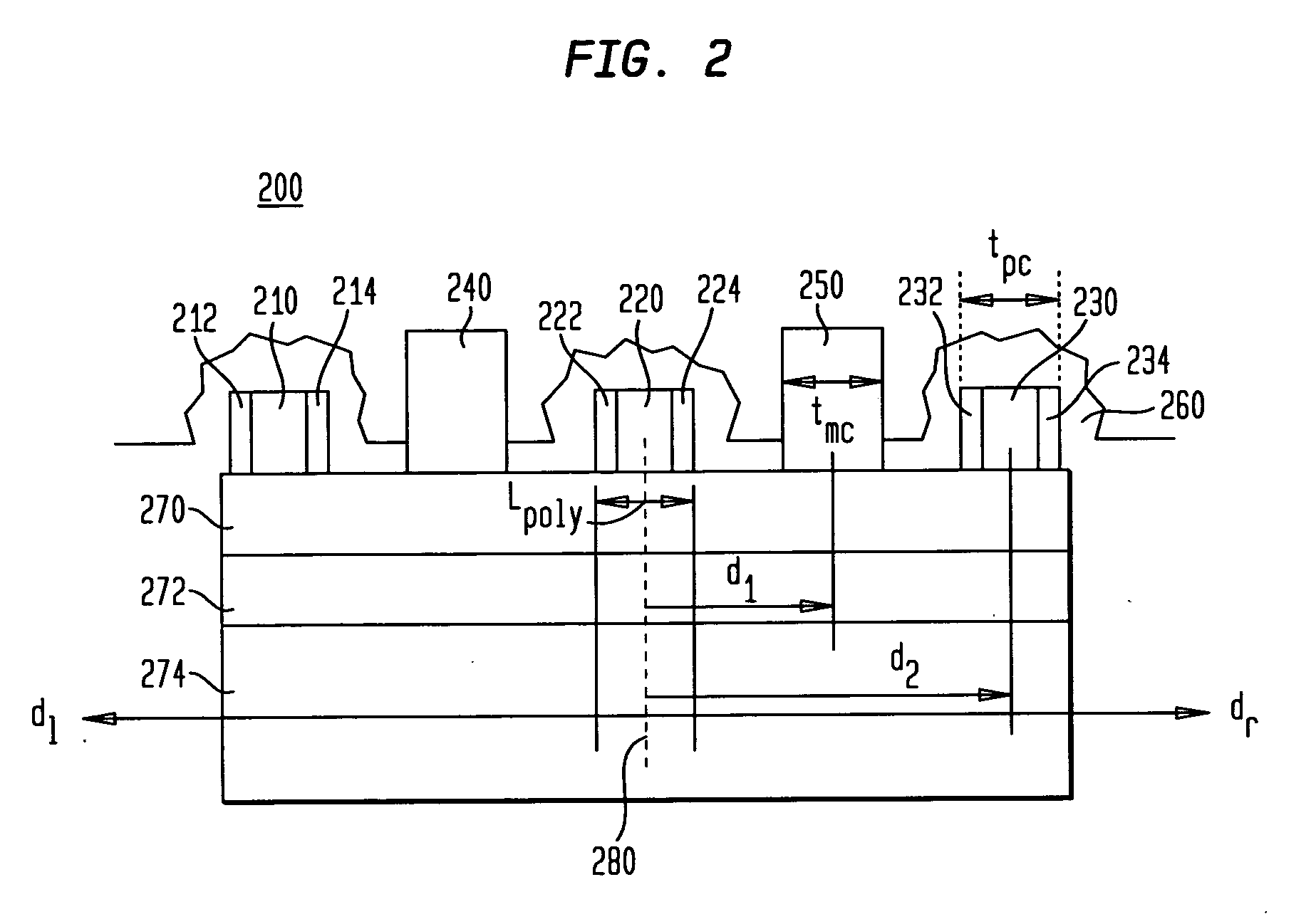
[0042] The present invention extends previously developed layout-sensitive compact model algorithms for other phenomena to accurately account for effects of layout-induced changes in nitride liner stress in semiconductor devices. In particular, the invention accounts for the impact of large layout variation on circuits with algorithms for obtaining the correct stress response approximations and layout extraction algorithms to obtain the correct geometric parameters that drive the stress response. Particularly, these algorithms include specific information in search “buckets” that are directionally-oriented and include directionally-specific distance measurements for analyzing in detail the specific shape neighborhood of the semiconductor device.

Analytical Model and Algorithm

[0043] It is problematic to interpolate experimentally-based results for all possible nitride liner case layouts because the layout variations are numerous and typical layout rules are either too complex or to...


PUM


Abstract

System and method for compact model algorithms to accurately account for effects of layout-induced changes in nitride liner stress in semiconductor devices. The layout-sensitive compact model algorithms account for the impact of large layout variation on circuits by implementing algorithms for obtaining the correct stress response approximations and layout extraction algorithms for obtaining the correct geometric parameters that drive the stress response. In particular, these algorithms include specific information from search “buckets” that are directionally-oriented and include directionally-specific distance measurements for analyzing in detail the specific shape neighborhood of the semiconductor device. The algorithms are additionally adapted to enable the modeling and stress impact determination of a device having single stress liner film and dual-stress liners (two different liner films that abut at an interface).

Description

BACKGROUND OF THE INVENTION [0001] 1. Field of Invention [0002] The invention relates to a technique for determining key transistor model quantities including device mobility for semiconductor devices and, more particularly to a technique for determining how these quantities are affected by the layout of a Semiconductor device that uses nitride liner films to apply stress in a transistor device channel. [0003] 2. Description of Related Art [0004] Stress can be applied in semiconductor devices to increase the mobility of electrons or holes in such devices. For example, stress can be applied to the channel of field effect transistors (FETs) by using intrinsically stressed films such as the liner film that is used normally in the formation of metal contact (MC) terminals to the source and drain regions of the FET. Stress films can typically be nitride films because nitride films are compatible with the silicon fabrication process steps used for contact formation and etching. Liner film...

Claims


Application Information

Patent Timeline
Patent Type & Authority Applications(United States)
IPC IPC(8): G06F17/50
CPCG06F17/5036H01L29/7843G06F17/5068G06F30/367G06F30/39
Inventor CHIDAMBARRAO, DURESETIJORDAN, DONALD L.MCCULLEN, JUDITH H.ONSONGO, DAVID M.WAGNER, TINAWILLIAMS, RICHARD Q.
Owner GLOBALFOUNDRIES US INC
Why Eureka
Try Eureka