Chalcogenide devices and materials having reduced germanium or telluruim content

a technology of germanium telluruim and chalcogenide, which is applied in the direction of bulk negative resistance effect devices, basic electric elements, electric devices, etc., can solve the problems of affecting the thermal stability of materials, and affecting the formation of chalcogenide, etc., to achieve favorable formation characteristics, short crystallization time, and favorable formation characteristics

Active Publication Date: 2007-02-15
OVONYX MEMORY TECH LLC
View PDF25 Cites 16 Cited by
  • Summary
  • Abstract
  • Description
  • Claims
  • Application Information

AI Technical Summary

Benefits of technology

[0013] In one embodiment, the instant invention provides chalcogenide alloy compositions that exhibit favorable formation characteristics along with short crystallization times. In another embodiment, the instant invention provides chalcogenide alloy compositions that exhibit crystallization times that vary only slightly over different structural states whose resistances extend over one or more orders of magnitude. When used in electrical chalcogenide device applications, the instant alloys provide for fast set speeds and / or favorable formation characteristics for a plurality of states that extend over a wide range of resistance. The instant alloys also provide favorable threshold voltages, reset currents, and reset resistances.

Problems solved by technology

A current issue in terms of the properties of chalcogenide materials is the need to improve the thermal stability of the materials.
Data in a chalcogenide material are retained as a structural state of the material, so any tendency of the structural state to transform with temperature represents a potential undesirable mechanism of erasing or losing data.
Many chalcogenide memory materials retain their structural states for long periods of time at room temperature, but become susceptible to variations in the structural state upon increasing temperature.
In practical terms, this limits the temperature environment in which chalcogenide memory devices can be utilized as well as the temperatures that can be employed in processing or manufacturing.

Method used


Image

  • Chalcogenide devices and materials having reduced germanium or telluruim content
  • Chalcogenide devices and materials having reduced germanium or telluruim content
  • Chalcogenide devices and materials having reduced germanium or telluruim content

Examples


example 1

[0045] In this example, the fabrication of memory devices having active chalcogenide layers in accordance with the instant invention is described. The device structure is a commonly utilized two-terminal device design having an active chalcogenide layer in a pore geometry in electrical contact with top and bottom electrodes. Two different device configurations were used and similar results were achieved for each. Both designs were deposited on a Si wafer with a thick SiO2 surface oxide layer.

[0046] In one design, a chalcogenide layer having a thickness of 500 Å was deposited on a circular lower electrode of dimension ≦1000 Å and having surrounding Sio2 layers. A top electrode was next deposited in situ and included a 400 Å carbon layer deposited on top of the chalcogenide layer and one or more conductive layers deposited on top of the carbon layer. The conductive layers typically included a 300 Å TiN layer and a 500 Å Ti layer. In a second design, a 350 Å bottom electrode layer (e....

example 2

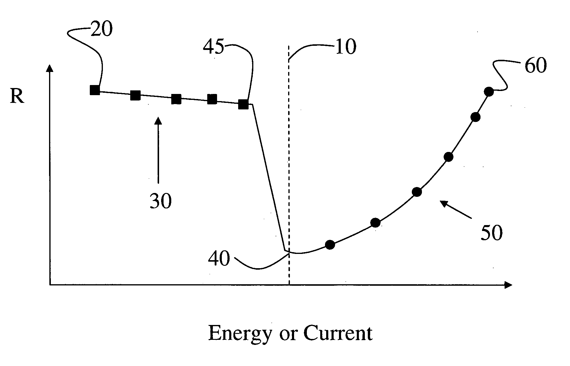
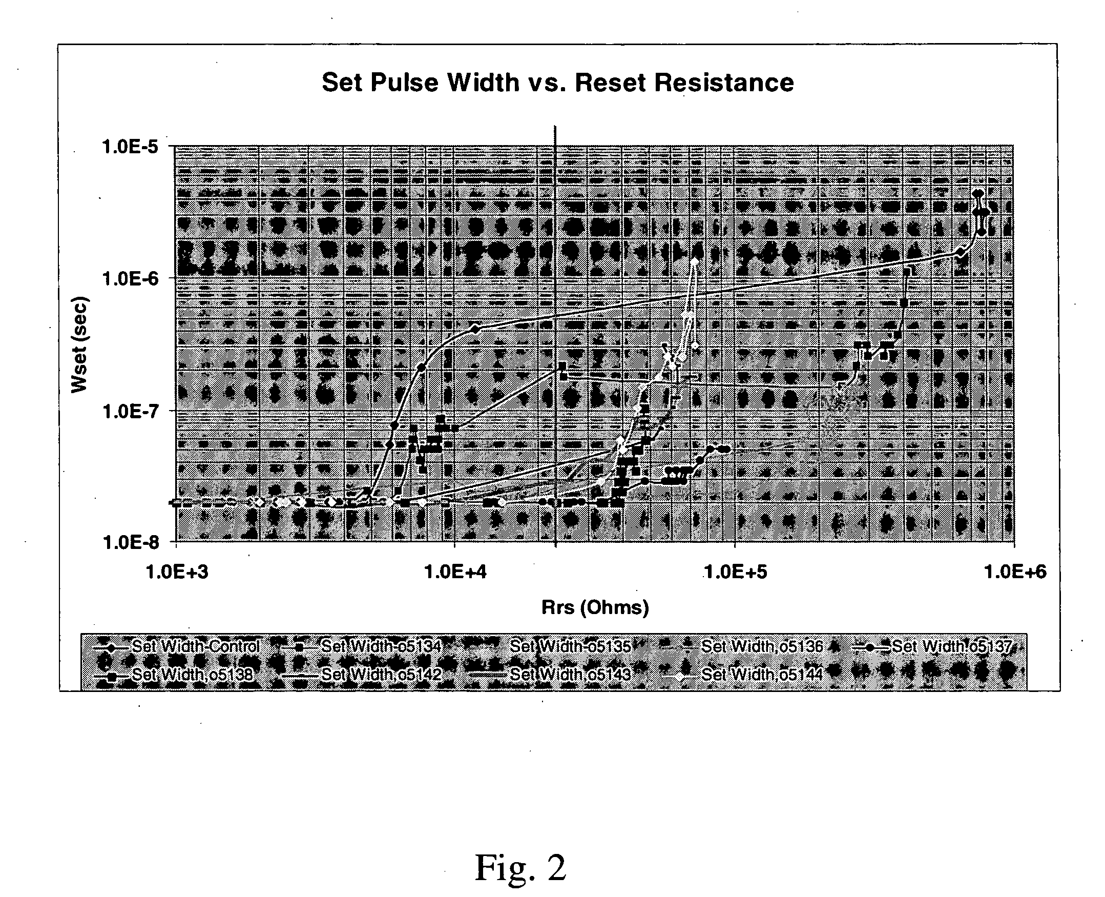
[0049] In this example; the improved crystallization speeds of devices that include chalcogenide materials according to the instant invention are described. The device structures utilized in this example correspond to those described in EXAMPLE 1 hereinabove. The crystallization speeds of devices including several of the chalcogenide compositions listed in EXAMPLE 1 hereinabove were measured. In the measurements, a current pulse was applied to the device to transform the chalcogenide to an initial state in the grayscale portion of the response curve. The resistance of the initial state was recorded. In the next step of the experiment, energy was applied to the device and the time required to set the device was recorded. The applied energy was in the form of a current pulse having a constant amplitude and variable width. The energy of the pulse was such that the device operated in the accumulating response regime of the resistance vs. current plot of the device (see FIG. 1). The resi...


PUM


Abstract

A chalcogenide material and chalcogenide memory device exhibiting fast operation (short set pulse times) over an extended range of reset state resistances. Electrical devices containing the instant chalcogenide materials permit rapid transformations from the reset state to the set state for reset and set states having a high resistance ratio. The instant devices thus provide for high resistance contrast and improved readability of memory states while preserving fast operational speeds for the device. The chalcogenide materials include materials comprising Ge, Sb and Te in which the Ge and/or Te content is lean relative to the commonly used Ge2Sb2Te5 chalcogenide composition. In one embodiment, the atomic concentration of Ge is between 11% and 22%, the atomic concentration of Sb is between 22% and 65%, and the atomic concentration of Te is between 28% and 55%. In a preferred embodiment, the atomic concentration of Ge is between 15% and 18%, the atomic concentration of Sb is between 32% and 35%, and the atomic concentration of Te is between 48% and 51%.

Description

RELATED APPLICATION INFORMATION [0001] This application is a continuation in part of U.S. patent application Ser. No. 11 / 200,466, entitled “Chalcogenide Devices Incorporating Chalcogenide Materials having Reduced Germanium or Tellurium Content”, filed on Aug. 9, 2005; the disclosure of which is hereby incorporated by reference herein.FIELD OF INVENTION [0002] This invention pertains to chalcogenide materials having utility in electrical memory or switching devices. More particularly, this invention is concerned with off-tieline chalcogenide alloys in the Ge—Sb—Te family that have a low Ge concentration and / or low Te concentration relative to the widely used Ge2Sb2Te5 alloy. Most specifically, this invention relates to electrical chalcogenide materials that exhibit high set speeds from initial states having high resistances. BACKGROUND OF THE INVENTION [0003] Chalcogenide materials are an emerging class of commercial electronic materials that exhibit switching, memory, logic, and pro...

Claims


Application Information

Patent Timeline
Patent Type & Authority Applications(United States)
IPC IPC(8): H01L47/00
CPCH01L45/06H01L45/1625H01L45/144H01L45/1233H10N70/231H10N70/026H10N70/826H10N70/8828
Inventor KOSTYLEV, SERGEY A.LOWREY, TYLERWICKER, GUYCZUBATYJ, WOLODYMYR
Owner OVONYX MEMORY TECH LLC
Why Eureka
Try Eureka