

Semiconductor device having an improved wiring or electrode structure
a semiconductor device and wire structure technology, applied in the field of semiconductor devices, can solve the problems of easy corrosion, change or deterioration of the characteristics of the semiconductor device, and relatively inferior mo in so as to improve the moisture resistance and corrosion resistance
- Summary
- Abstract
- Description
- Claims
- Application Information
AI Technical Summary
Benefits of technology
Problems solved by technology
Method used
Image

Examples
first embodiment
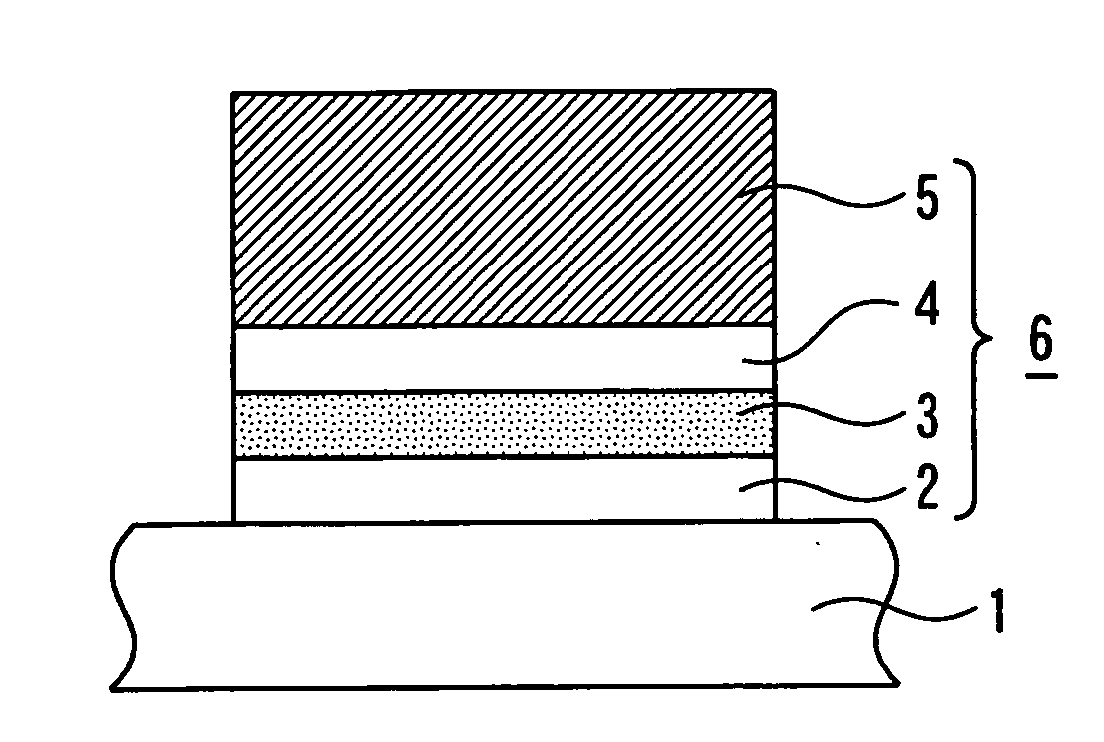
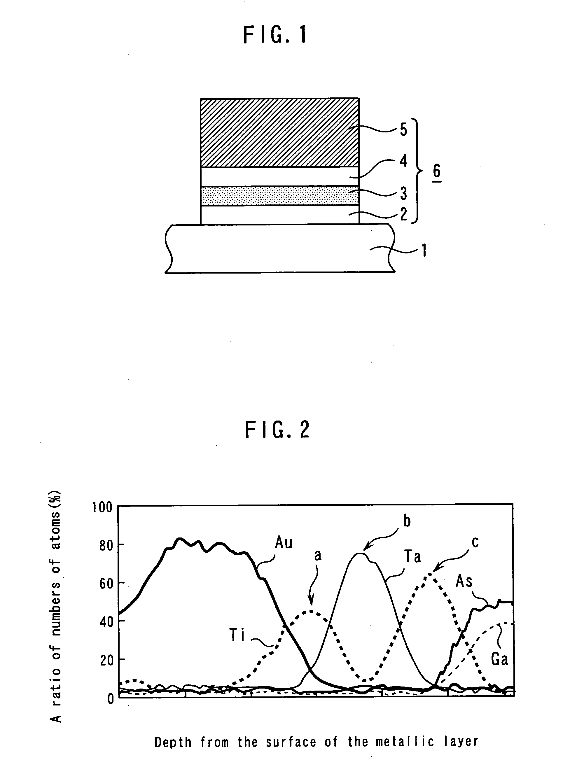
[0019] A cross-sectional structure of a semiconductor device according to a first embodiment is shown in FIG. 1. This is a cross-sectional structure of an ohmic electrode formed on a p-type GaAs layer. A p-type GaAs layer 1 is formed on a GaAs substrate (not shown). Thereon, a lower Ti layer 2 (film thickness of about 50 nm), a diffusion preventing layer 3 (film thickness of about 50 nm), an upper Ti layer 4 (film thickness of about 50 nm), and a metallic layer 5 (film thickness of about 250 nm) are formed. Hereafter, a stacked film formed of the lower Ti layer 2, the diffusion preventing layer 3, the upper-Ti layer 4, and the metallic layer 5 is referred to as an “ohmic electrode”6. The ohmic electrode 6 having a predetermined width is formed on the p-type GaAs layer 1. As the diffusion preventing layer 3, tantalum (Ta) is used, and as the metallic layer 5, gold (Au) is used.
[0020] In other words, in the above-described structure, a diffusion preventing layer 3 consisting of Ta is...
second embodiment
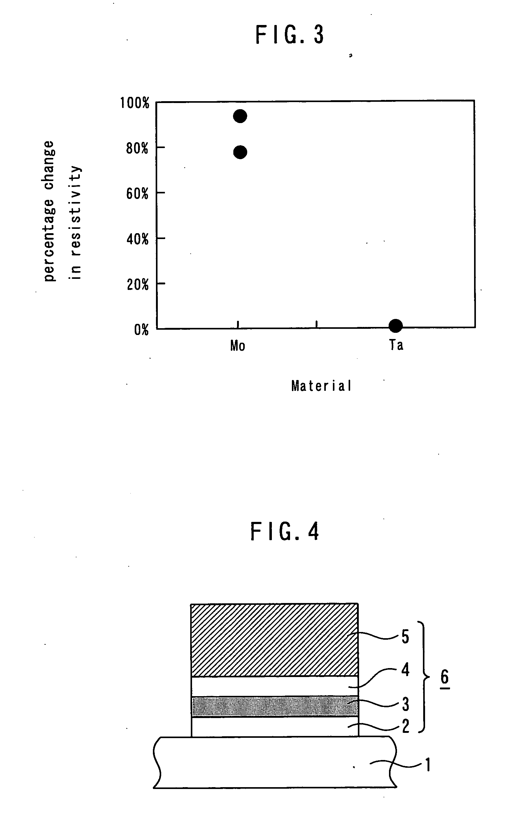
[0032] A cross-sectional structure of a semiconductor device according to a second embodiment is shown in FIG. 4. Here, the second embodiment is described focusing on the aspects different from the first embodiment. In the structure, as in the first embodiment, an ohmic electrode is formed on a p-type GaAs layer. In the second embodiment, the structure using an alloy film formed of Mo and Nb is used as a diffusion preventing layer 3. Since other constitutions are equivalent to those of the first embodiment, the description thereof will be omitted.
[0033] By using an alloy film formed of Mo and Nb as the diffusion preventing layer 3, in the same way as in the case wherein Mo or Nb is used alone, the interdiffusion of Ga and As in the p-type GaAs layer 1, and Au in the metallic layer 5 can be effectively suppressed.
[0034] Next, moisture resistance when an alloy film formed of Mo and Nb is used as the diffusion preventing layer 3 will be described.
[0035] First, a sample wherein an al...
third embodiment
[0045] A cross-sectional structure of a semiconductor device according to a third embodiment is shown in FIG. 6. Here, the third embodiment is described focusing on the aspects different from the first and second embodiments. FIG. 6 shows a cross-sectional structure of a Schottky electrode formed on an n-type GaAs layer, and a wiring formed thereon.
[0046] An n-type GaAs layer 8 is formed on a substrate (not shown). On the n-type GaAs layer 8, a Ti film 9 (film thickness of about 50 nm) and a first metallic layer 10 (film thickness of about 500 nm) are formed in predetermined widths (hereafter, the stacked film formed of the Ti film 9 and the first metallic layer 10 is referred to as “Schottky electrode 11”). As the first metallic layer 10, aluminum (Al) is used.
[0047] On the Schottky electrode 11, a lower Ti layer 12 (film thickness of about 50 nm), a diffusion preventing layer 13 (film thickness of about 50 nm), an upper Ti layer 14 (film thickness of about 50 nm), and a second m...
PUM
 Abstract
Description
Claims
Application Information