Successive approximation A/D converter

Active Publication Date: 2007-02-15
CYPRESS SEMICON CORP
View PDF5 Cites 41 Cited by
  • Summary
  • Abstract
  • Description
  • Claims
  • Application Information

AI Technical Summary

Benefits of technology

[0039] According to at least one embodiment of the present invention, a sample-hold amplifier circuit having the voltage gain smaller than 1 and a switched capacitor D/A converter that samples the outputs of the sample-hold amplifier circuit are provided. With this provision, a potential difference proportional to the analog input potential difference can be supplied from the amplifier circuit to the switched capacitor D/A converter

Problems solved by technology

In the related-art configuration as shown in FIG. 1, however, the sampling capacitors are charged by use of the external analog input signals, so that the sampling time is limited by the capacitance of the sampling capacitors.
It is thus difficult to shorten the sampling time suff

Method used


Image

  • Successive approximation A/D converter
  • Successive approximation A/D converter
  • Successive approximation A/D converter

Examples


Embodiment Construction

[0068] In the following, embodiments of the present invention will be described with reference to the accompanying drawings.

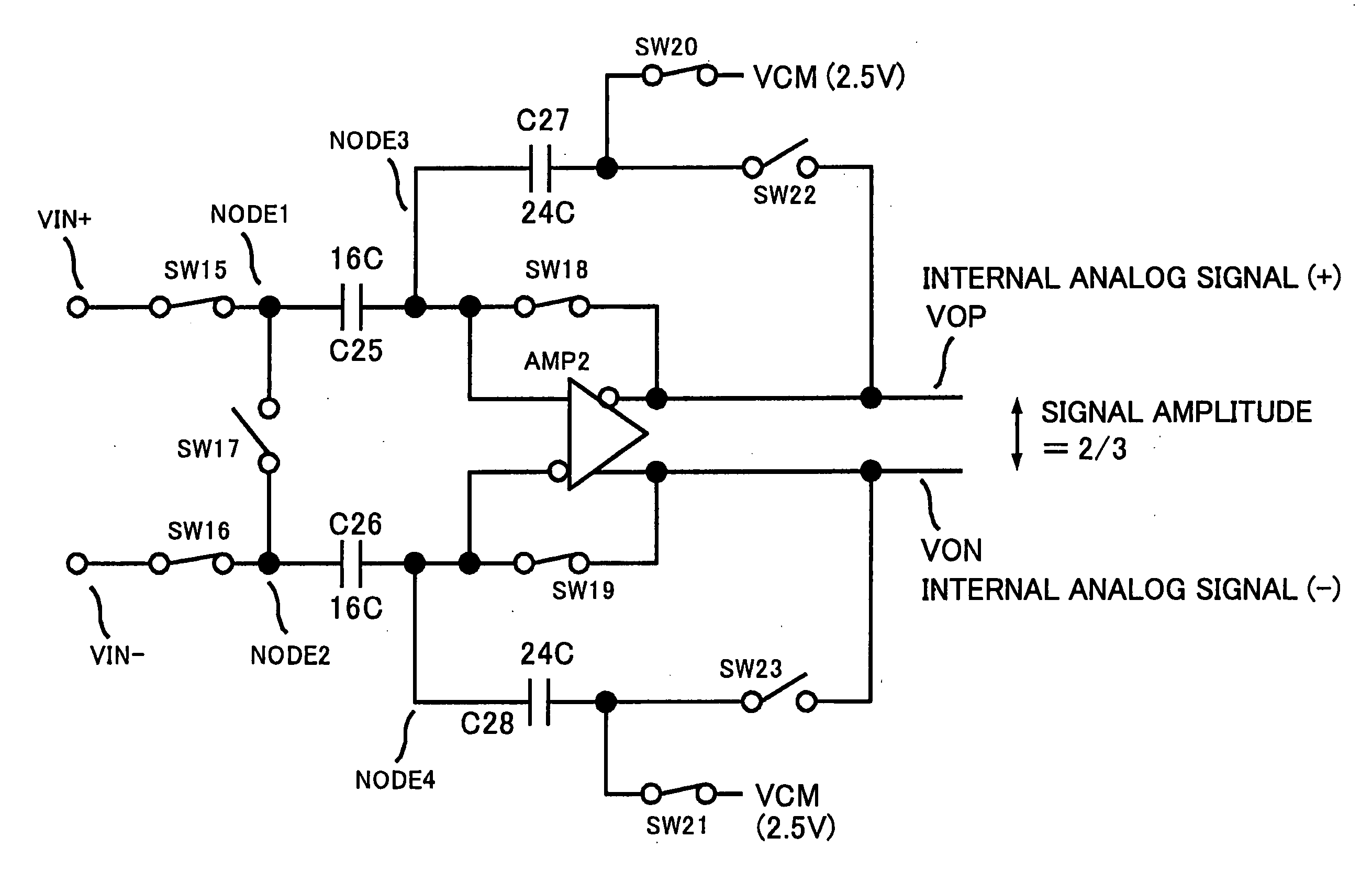
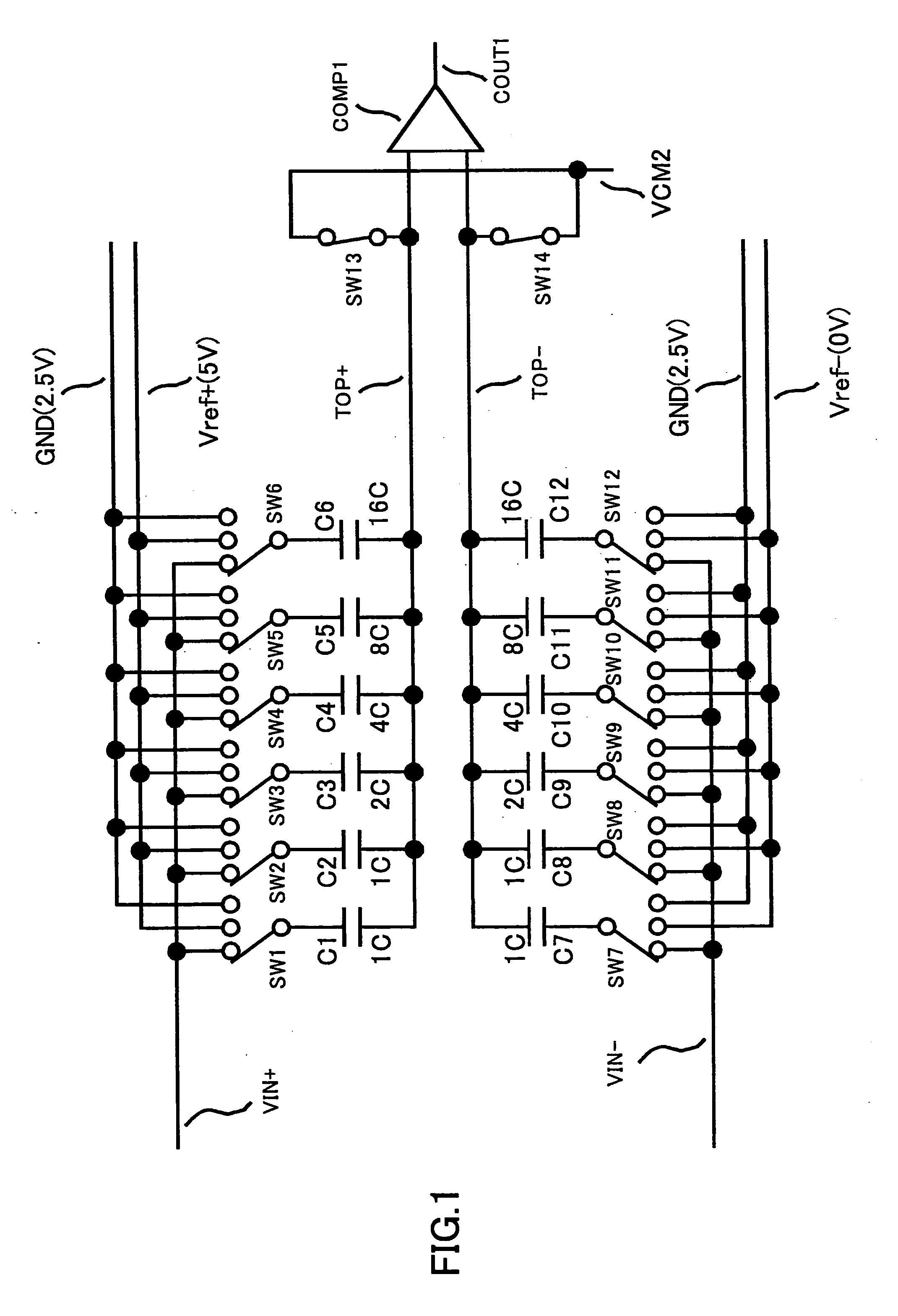
[0069]FIGS. 5A and 5B are circuit diagrams showing a first embodiment of a successive approximation A / D converter according to the present invention. FIG. 5A illustrates a circuit portion corresponding to a sample-hold amplifier circuit, and FIG. 5B illustrates a circuit portion corresponding to a capacitor array unit that is coupled to the output of the sample-hold amplifier circuit. The output of the capacitor array unit is coupled to a comparator in the same manner as shown in FIG. 1.

[0070] The circuit shown in FIGS. 5A and 5B includes switches SW13, SW14, SW15 through SW23, and SW27 through SW42, capacitors C25 through C28, capacitors C30 through C45, and an amplifier circuit AMP2. VIN+ is a plus-side analog input potential, and VIN− is a minus-side analog input potential. VOP and VON are plus-side and minus-side internal analog signals, respectively, whi...


PUM


Abstract

A successive approximation. A/D converter includes a sample-hold amplifier circuit configured to sample and hold an input analog voltage to produce an internal analog voltage proportional to the input analog voltage with a voltage gain being smaller than 1, a switched capacitor D/A converter coupled to the sample-hold amplifier circuit and including a plurality of capacitors for storing electric charge responsive to the internal analog voltage, the switched capacitor D/A converter configured to switch couplings of the capacitors in response to a control signal to produce a comparison analog voltage responsive to the internal analog voltage and the control signal, a comparator coupled to the switched capacitor D/A converter to produce a comparison result signal responsive to the comparison analog voltage, and a control circuit coupled to the comparator to supply the control signal responsive to the comparison result signal to the switched capacitor D/A converter.

Description

CROSS-REFERENCE TO RELATED APPLICATIONS [0001] The present application is based upon and claims the benefit of priority from the prior Japanese Patent Application No. 2005-234724 filed on Aug. 12, 2005, with the Japanese Patent Office, the entire contents of which are incorporated herein by reference. BACKGROUND OF THE INVENTION [0002] 1. Field of the Invention [0003] The present invention generally relates to successive approximation A / D converters, and particularly relates to a successive approximation A / D converter utilizing a switched capacitor D / A converter. [0004] 2. Description of the Related Art [0005] Successive approximation A / D converters can be implemented by use of relatively simple circuit configurations, and can be manufactured at relatively low cost due to their suitability for CMOS process while providing moderate conversion time and moderate conversion accuracy. This is why successive approximation A / D converters are used in a variety of fields. FIG. 1 is a drawing...

Claims


Application Information

Patent Timeline
IPC IPC(8): H03M1/38
CPCH03M1/468H03M1/0682H03M1/38
Inventor TACHIBANA, SUGURUMITSUDA, KAZUHIROKATO, TATSUO
Owner CYPRESS SEMICON CORP
Why Eureka
Try Eureka