Scintillator panel, scintillator panel laminate, radiation image sensor using the same, and radiation energy discriminator

a scintillator and scintillator technology, applied in the direction of fluorescence/phosphorescence, radiation controlled devices, optical radiation measurement, etc., can solve the problems of inability to say high detection precision, complicated procedures for obtaining incidence energy, and inherently limited thickness of scintillator, etc., to achieve high deliquescence properties, prevent obstruction of x-rays and other radiation incidents, and high strength

Inactive Publication Date: 2007-02-22
HAMAMATSU PHOTONICS KK
View PDF9 Cites 27 Cited by
  • Summary
  • Abstract
  • Description
  • Claims
  • Application Information

AI Technical Summary

Benefits of technology

[0021] Also, by setting the substrate made of a metal material, a scintillator member of high strength can be obtained. Also by setting the substrate made of a metal material, the light emitted from the scintillator can propagate and be guided by reflection between substrate surfaces.
[0022] By setting the substrate made of a carbon-based material, the obstruction of X-rays and other radiation incident can be prevented.
[0023] Furthermore, by forming a protective film on the surfaces of the scintillator, the scintillator can be protected from physical and chemical damage due to external causes.
[0024] Scintillator has generally high deliquescence properties and degrade easily when water becomes attached. By the protective film having a moisture-proof property, contact of the scintillators with water can be prevented favorably. Deliquescence of the scintillator can thus be prevented favorably.
[0025] Also by forming a reflecting film on the surfaces of the scintillator, the light emitted from the scintillator generated by the scintillation emission due to radiation incident can be prevented from leaking outside the scintillator member and the light amount of the detected light can be made large.
[0026] Meanwhile, the stacked scintillator panel of the present invention is formed by stacking a plurality of any of the above-described scintillator panels. For the same scintillator thickness, the number of scintillator panels in the interior can be reduced and the thickness of the laminate as a whole can also be reduced.

Problems solved by technology

With the radiation image sensor described in Document 1, though a columnar scintillator is formed on a substrate, the thickness of the scintillator that can be formed is inherently limited.
With the energy discriminator described in Patent Document 2, since the incidence energy of radiation is estimated from the spatial spread on the image pickup element that detects the scintillator emission, the procedures for obtaining the incidence energy are complicated and yet the detection precision cannot be said to be high.

Method used


Image

  • Scintillator panel, scintillator panel laminate, radiation image sensor using the same, and radiation energy discriminator
  • Scintillator panel, scintillator panel laminate, radiation image sensor using the same, and radiation energy discriminator
  • Scintillator panel, scintillator panel laminate, radiation image sensor using the same, and radiation energy discriminator

Examples


first embodiment

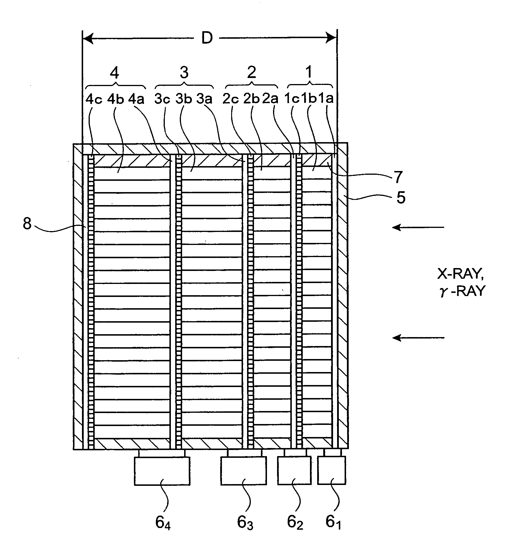
[0038]FIG. 1 shows the present invention, which is a radiation energy discriminator using a scintillator panel.

[0039] In FIG. 1, the energy discriminator comprises four panels 1, 2, 3, and 4 (having scintillator 1b, 2b, 3b, and 4b, respectively), which receive radiation, a protective film 5, which covers entire panels 1, 2, 3, and 4, respectively, to prevent absorbing moisture by the scintillator 1b, 2b, 3b, and 4b, solid linear sensors or other photodetectors 61, 62, 63, and 64, which are respectively connected to end portions at one side of substrates 1a, 2a, 3a, and 4a for crystal deposition in the panels 1, 2, 3, and 4 and respectively detect the light emitted from the scintillator 1b, 2b, 3b, and 4b upon incidence of radiation, and supporting films 7, which are disposed at the end portions at the other side of the substrates 1a, 2a, 3a, and 4a for crystal deposition to support side face portions of the scintillator 1b, 2b, 3b, and 4b.

[0040] The panels 1, 2, 3, and 4 have a com...

second embodiment

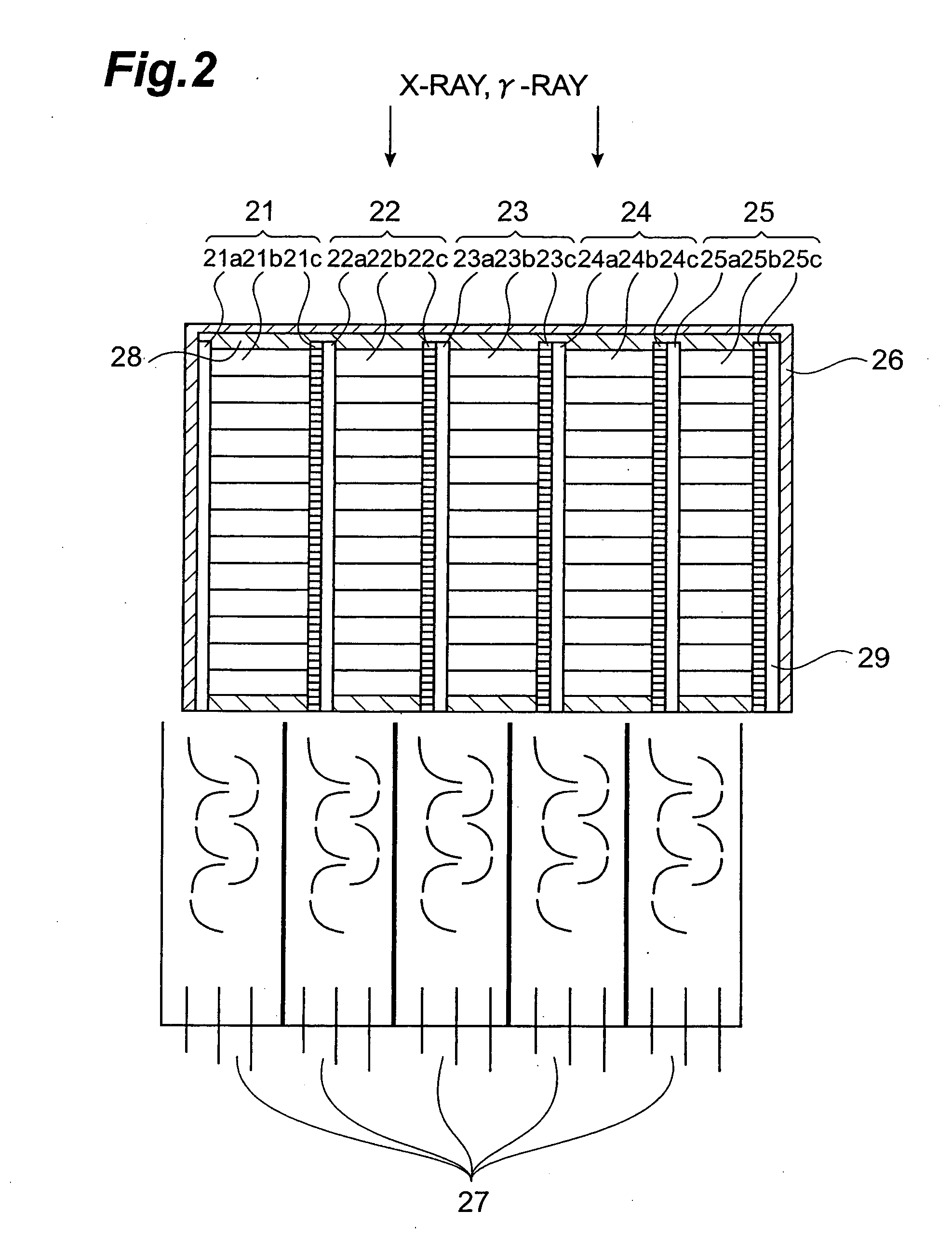
[0059]FIG. 2 shows the present invention and is a sectional view of a radiation image sensor that uses scintillator panel of the present invention. The image sensor comprises five panels 21, 22, 23, 24, and 25 (respectively having scintillator 21b, 22b, 23b, 24b, and 25b which convert radiation to visible light) onto which radiation enters, a protective film 26, which covers the entire panels 21, 22, 23, 24, and 25 to prevent moisture absorption by the scintillator 21b, 22b, 23b, 24b, and 25b, photoelectric converters 27, comprising of photomultiplier tubes connected to end portions at one side of the substrates 21a, 22a, 23a, 24a, and 25a for crystal deposition inside the panels 21, 22, 23, 24, and 25 and obtain electrical signals by detecting the respective emitted light generated in the scintillator 21b, 22b, 23b, 24b, and 25b upon radiation incidence, and supporting films 28, disposed at the end portions at the other side of the substrates 21a, 22a, 23a, 24a, and 25a for crystal...

third embodiment

[0069] Also, in the case where the scintillator panel according to the present invention is used in an image sensor, a CCD or other image pickup element may be used without the use of photoelectric converters that comprise photomultiplier tubes, etc. To describe an example using an image pickup element with reference to a third embodiment, illustrated in FIG. 3, the same scintillator panel as that shown in FIG. 2 is used, and a CCD 30 is mounted to end portions at one side of the respective substrates 21b to 25b for crystal deposition of the panels 21 to 25 of this scintillator panel. With this embodiment, an image is formed not upon conversion of light to electrons by photomultiplier tubes or other photoelectric converters but the light that arrives upon propagating through the substrates 21b to 25b for crystal deposition can be picked up as they are by the CCD camera.


PUM


Abstract

The stacked scintillator panel according to the present invention is comprised of stacking a plurality of panels 1, 2, 3, 4, having scintillator 1b, 2b, 3b, and 4b deposited by vapor deposition on substrates 1a, 2a, 3a, and 4a for crystal deposition. Each of the substrates 1a, 2a, 3a, and 4a is a light transmitting substrate that transmits at least a portion of the wavelength range of the light emitted from the corresponding scintillator 1b, 2b, 3b, or 4b upon radiation incidence.

Description

TECHNICAL FIELD [0001] The present invention is related to a scintillator panel, a laminated scintillator panel, and a radiation image sensor and a radiation energy discriminator using the same, which are used for detecting and image taking of X-rays, γ-rays, etc., in medical and industrial applications. BACKGROUND ART [0002] As an example of an image sensor for X-rays, γ-rays, etc. (referred to hereinafter as “radiation”), the device described in International Patent Publication No. WO 99 / 66345 Pamphlet (referred to hereinafter as “Document 1”) is known. FIG. 9 shows such an example of a radiation image sensor. This radiation image sensor comprises a substrate 60 made of amorphous carbon (a-C) having sandblasted surface, an Al film 62 formed on one surface of the substrate 60 as a light reflecting film, and a scintillator 64 consisted of TI-doped CsI with needle-like structures formed on the surface of the Al film 62. The structure comprising the substrate 60, the Al film 62, and t...

Claims


Application Information

Patent Timeline
Patent Type & Authority Applications(United States)
IPC IPC(8): G01T1/20G01T1/36H01L27/14H01L27/146H01L31/0232H01L31/09H04N5/32H04N5/335H04N5/369
CPCH01L31/02322H01L27/14663G01T1/20
Inventor SATO, HIROTOSUZUKI, TAKAHARU
Owner HAMAMATSU PHOTONICS KK
Why Eureka
Try Eureka