Method for the removal of deposition on an optical element, method for the protection of an optical element, device manufacturing method, apparatus including an optical element, and lithographic apparatus

a technology for optical elements and removal methods, applied in the direction of lithographic apparatus, cleaning process and apparatus, and printing, etc., can solve the problems of collector mirror sputtering, collector mirror sputtering is particularly problematic, and other mirrors in the system are generally damaged to a lesser degree, so as to improve the removal

Inactive Publication Date: 2007-02-22
ASML NETHERLANDS BV
View PDF3 Cites 41 Cited by
  • Summary
  • Abstract
  • Description
  • Claims
  • Application Information

AI Technical Summary

Benefits of technology

[0011] In another embodiment, the deposition includes one or more elements selected from B, C, Si, Ge and Sn. C (carbon) may, for example, be a deposition on the optical element due to the undesired presence of hydrocarbons in the apparatus, like a lithographic apparatus, but may also be deliberately present as protective cap layer. Si (silicon) may also be deliberately present as protective cap layer, whereas Sn (tin) may be present due to a source that produces Sn. Further, Si may be present as deposition due to outgassing of the resist. In a further embodiment, at least part of the hydrogen radicals are generated from H2 from the H2 containing gas by one or more radical formation devices selected from a hot filament, a plasma, radiation, and a catalyst for converting H2 into hydrogen radicals. The hydrogen radical reacts with Sn (or Sn oxides), C, Si (or Si oxides), etc., leading to volatile hydrides that can be removed by, for example, an exhaust. Sn and Si, that may have oxidized or which may be at least partially present as oxide as deposition or cap layer may be reduced to elemental Sn and Si, respectively, and may be removed as hydride or as halogenide. Therefore, in yet another embodiment, the H2 containing gas may further include a halogen gas. The halogens may form volatile halides, and may improve the removal of e.g. Sn and Si deposition.

Problems solved by technology

These particles can be damaging to the collector and condenser mirrors which are generally multilayer mirrors, with fragile surfaces.
The sputtering effect is particularly problematic for the collector mirror.
Other mirrors in the system are generally damaged to a lesser degree by sputtering of particles expelled from the plasma since they may be shielded to some extent.

Method used


Image

  • Method for the removal of deposition on an optical element, method for the protection of an optical element, device manufacturing method, apparatus including an optical element, and lithographic apparatus
  • Method for the removal of deposition on an optical element, method for the protection of an optical element, device manufacturing method, apparatus including an optical element, and lithographic apparatus
  • Method for the removal of deposition on an optical element, method for the protection of an optical element, device manufacturing method, apparatus including an optical element, and lithographic apparatus

Examples


Embodiment Construction

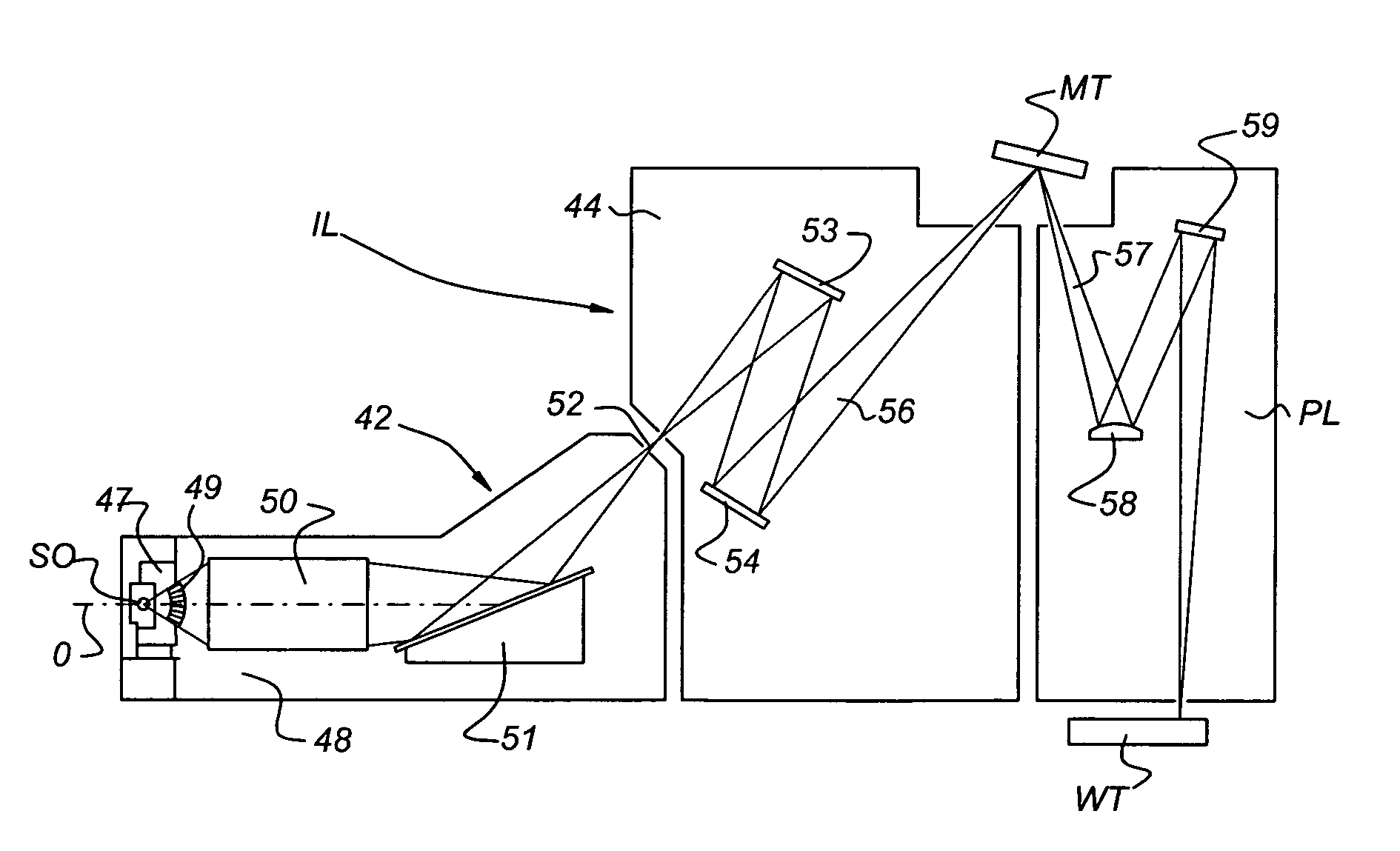
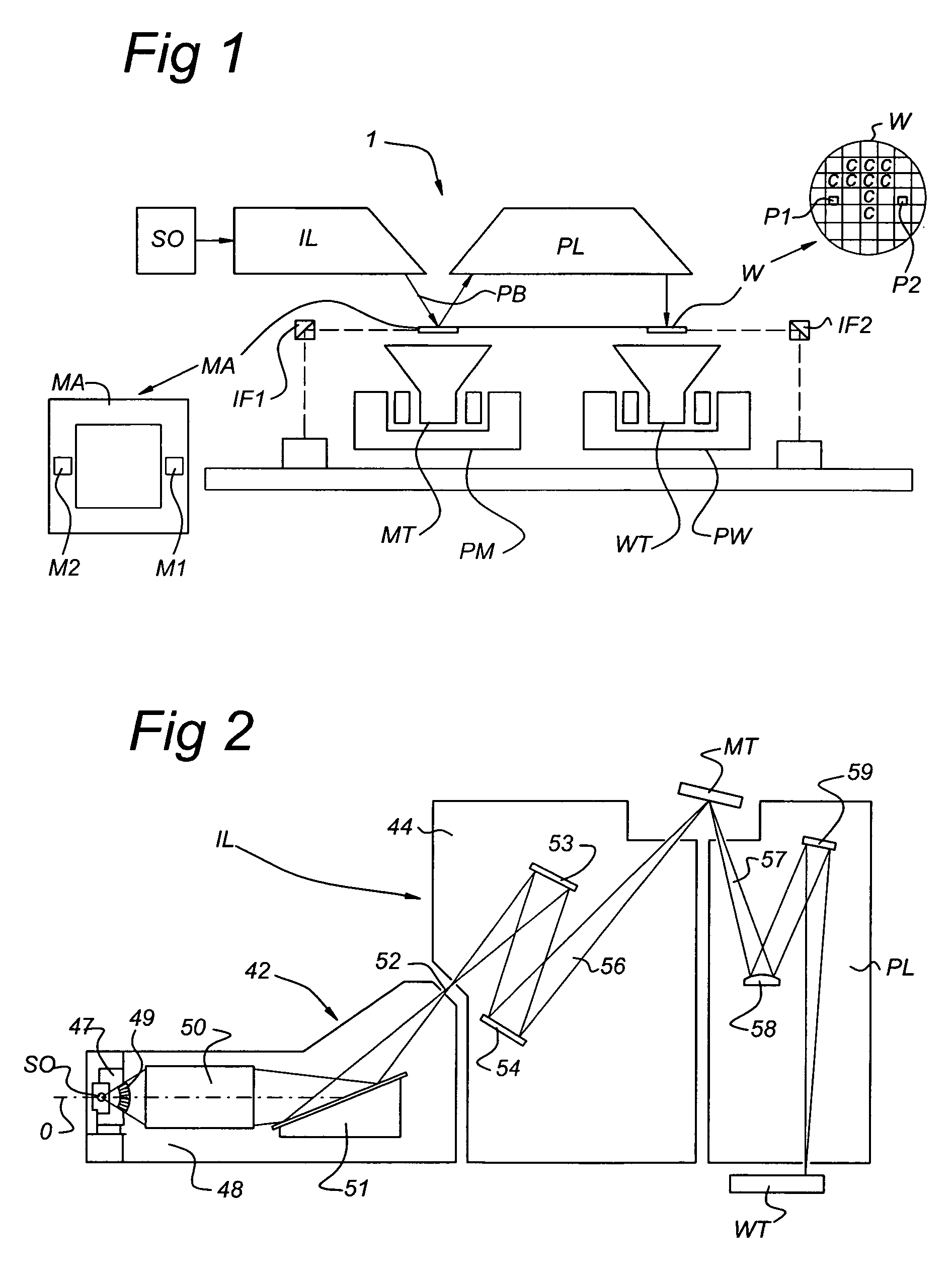
[0057]FIG. 1 schematically depicts a lithographic apparatus 1 according to an embodiment of the present invention. The apparatus 1 includes an illumination system (illuminator) IL configured to condition a radiation beam B (e.g. UV radiation or EUV radiation). A support (e.g. a mask table) MT is configured to support a patterning device (e.g. a mask) MA and is connected to a first positioning device PM configured to accurately position the patterning device in accordance with certain parameters. A substrate table (e.g. a wafer table) WT is configured to hold a substrate (e.g. a resist-coated wafer) W and is connected to a second positioning device PW configured to accurately position the substrate in accordance with certain parameters. A projection system (e.g. a refractive projection lens system) PL is configured to project the patterned radiation beam B onto a target portion C (e.g. including one or more dies) of the substrate W.

[0058] The illumination system may include various ...


PUM

PropertyMeasurementUnit
wavelengthaaaaaaaaaa
wavelengthsaaaaaaaaaa

Abstract

A method for the removal of a deposition on an optical element of an apparatus including the optical element includes providing an H2 containing gas and one or more additional compounds selected from the group of hydrocarbon compounds and silane compounds in at least part of the apparatus includes producing hydrogen radicals from H2 from the H2 containing gas; and bringing the optical element with deposition into contact with at least part of the hydrogen radicals and removing at least part of the deposition. Further, a method for the protection of an optical element of an apparatus including the optical element includes providing a cap layer to the optical element by a deposition process; and during or after use of the apparatus, removing at least part of the cap layer from the optical element in a removal process as described above. The methods can be applied in a lithographic apparatus.

Description

BACKGROUND OF THE INVENTION [0001] 1. Field of the Invention [0002] The present invention relates to a method for the removal of deposition on an optical element, a method for the protection of an optical element, a device manufacturing method, an apparatus including an optical element, and a lithographic apparatus. [0003] 2. Description of the Related Art [0004] A lithographic apparatus is a machine that applies a desired pattern onto a substrate, usually onto a target portion of the substrate. A lithographic apparatus can be used, for example, in the manufacture of integrated circuits (ICs). In that example, a patterning device, which is alternatively referred to as a mask or a reticle, may be used to generate a circuit pattern to be formed on an individual layer of the IC. This pattern can be transferred onto a target portion (e.g. including part of, one, or several dies) on a substrate (e.g. a silicon wafer). Transfer of the pattern is typically via imaging onto a layer of radia...

Claims


Application Information

Patent Timeline
Patent Type & Authority Applications(United States)
IPC IPC(8): B08B6/00
CPCG03F7/70925
Inventor WILHELMUS VAN HERPEN, MAARTEN MARINUS JOHANNESSPEE, CAROLUS IDA MARIA ANTONIUSKLUNDER, DERK JAN WILFREDDE MOL, ANTONIUS MARIA BERNARDUS
Owner ASML NETHERLANDS BV
Why Eureka
Try Eureka