Apparatus for fabricating a display device

a display device and apparatus technology, applied in the direction of non-linear optics, identification means, instruments, etc., can solve the problems of irradiation of necessary parts, silicon melts and undergoes aggregation, and thermal damage to the substrate, so as to prevent the occurrence of melting or aggregation of silicon film, prevent thermal damage to the glass substrate, and prevent the effect of irradiation high precision

Inactive Publication Date: 2007-02-22
PANASONIC LIQUID CRYSTAL DISPLAY CO LTD +1
View PDF29 Cites 16 Cited by
  • Summary
  • Abstract
  • Description
  • Claims
  • Application Information

AI Technical Summary

Benefits of technology

[0023] With the invention, while the stage is kept in continuous movement, only necessary pats can be irradiated with the laser light by turning the continuous-wave laser light ON / OFF, and parts where the laser irradiation is not required will not be irradiated, so that occurrence of melting or aggregation of the silicon film can be prevented. Also, it is possible to prevent thermal damage to a glass substrate etc. as the thin-film transistor substrate. Further, since the start and stoppage of the laser light irradiation can be controlled on the basis of the position of the stage, high precision irradiation start and stop is ensured even there occurs variation in the moving speed of the stage.

Problems solved by technology

However, according to the conventional techniques described in [Non-patent Document 1], irradiation is performed by scanning the whole surface of a region on the substrate, for forming a driver circuit, with the continuous wave laser, and no consideration is given to an idea of irradiation of necessary parts only.
As a result, after start of laser irradiation, laser absorbed by a silicon film is converted into heat, and accumulated in the substrate, so that the silicon melts and undergoes aggregation by the agency of interfacial tension or thermal damage occurs to the substrate.
So, this has been one the pending problems.
However, no thought has been given to a method of irradiating laser light to a specific spot on a substrate being moved at a high speed relative to laser.
This has been another problem to be solved.

Method used


Image

  • Apparatus for fabricating a display device
  • Apparatus for fabricating a display device
  • Apparatus for fabricating a display device

Examples


Embodiment Construction

[0061] Embodiments of the invention are described in detail hereinafter with reference to the accompanying drawings.

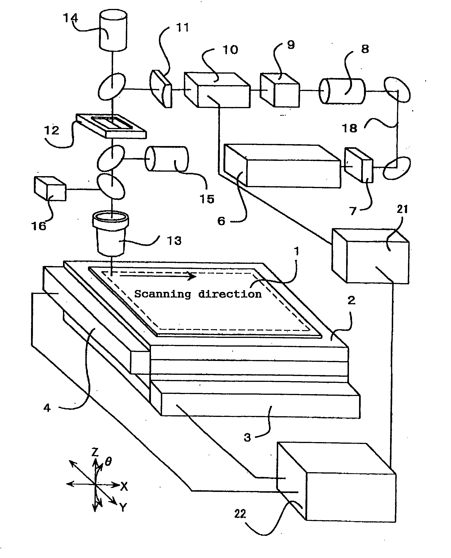
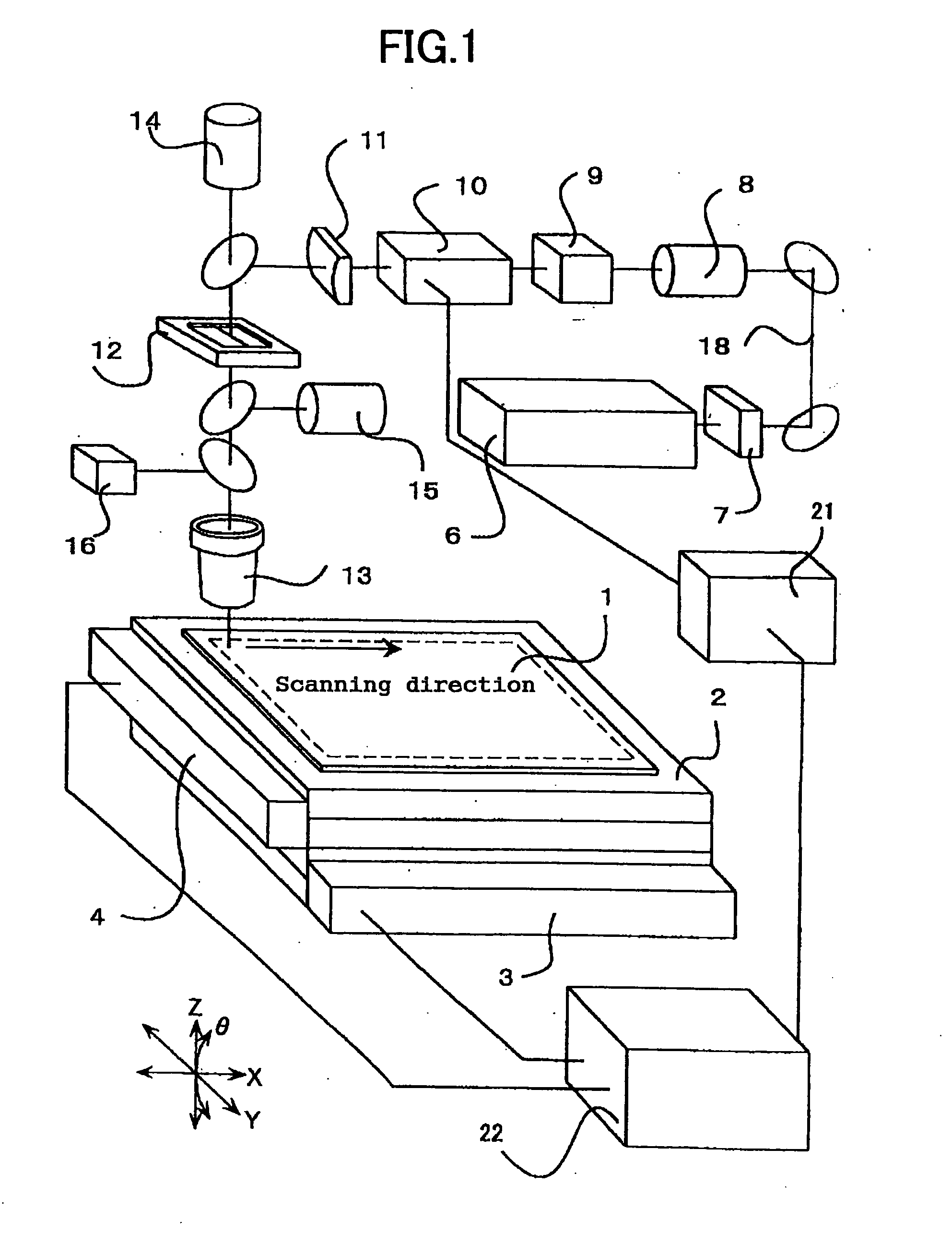
[0062]FIG. 1 is a block diagram for schematically illustrating an embodiment of an apparatus of fabricating a display device according to the invention for carrying out an embodiment of a process of fabricating the display device according to the invention. In this case, for an insulating substrate to serve as a thin-film transistor substrate, a glass substrate is used. A glass substrate 1 is movable in one direction (X) and in another direction (Y) crossing the one direction (X) at right angles, and is placed on a XYθ stage 2 (hereinafter referred to merely as stage) capable of adjusting both the directions (θ). The stage 2 fixedly attached to a platen (not shown) having a vibration isolation mechanism is provided with linear scales (also referred to as linear encoders) 3, 4, for detecting coordinates in the X direction and the Y direction, respectively.

[0063] A las...


PUM

PropertyMeasurementUnit
grain sizeaaaaaaaaaa
diameteraaaaaaaaaa
diameteraaaaaaaaaa

Abstract

Apparatus for fabricating a display device includes a stage capable of mounting an insulating substrate of the display device and moving the insulating substrate, linear scales which detect a position or moving distance of the substrate, a laser oscillator which generates continuous-waves laser light, a modulator which turns ON / OFF the continuous-wave laser light, a beam forming optic which shapes the continuous-wave laser light passing through the modulator into a linear or rectangular form, an objective lens which projects the at least one of the laser light on the insulating substrate so as to irradiate the insulating substrate with the laser light. The controller counts signals generated by the linear scales for every movement of the stage for a given distance, causes the modulator to turn the generated continuous-wave laser light in an ON state at time when a position of the insulating substrate on which the laser light irradiation is to be started reaches an area on which the laser light is projected, and causes the modulator to turn the generated continuous-wave laser light in an OFF state at another time.

Description

CROSS REFERENCE TO RELATED APPLICATION [0001] This is a continuation of U.S. application Ser. No. 10 / 628,421, filed Jul. 29, 2003. This application relates to and claims priority from Japanese Patent Application No. 2002-256533, filed on Sep. 2, 2002 and No. 2003-062938, filed on Mar. 10, 2003. The entirety of the contents and subject matter of all of the above is incorporated herein by reference. BACKGROUND OF THE INVENTION [0002] 1. Field of the Invention [0003] The present invention relates to a flat panel display device, and in particular, to a display device using an insulating substrate with active elements formed in a band-like polycrystalline semiconductor film, obtained by reforming an amorphous or granular polycrystalline semiconductor film formed on the top surface of the insulating substrate so as to expand crystal grains into a substantially band-like shape by use of annealing with laser light (also referred to merely as laser hereinafter) irradiated thereto to, a proce...

Claims


Application Information

Patent Timeline
Patent Type & Authority Applications(United States)
IPC IPC(8): H01S3/10G02B27/10G02F1/1368G02F1/13G09F9/30G09F9/35H01L21/20H01L21/268H01L21/336H01L21/77H01L21/84H01L27/32H01L29/04H01L29/786H01L51/50H05B33/02H05B33/10
CPCH01L21/2026H01L21/268H01L29/04H01L21/0268H01L27/1285H01L21/02691H01L21/02683H01L29/66757H01L21/02686H01L21/02678H01L21/02488H01L21/02422H01L21/02532H01L21/02595G02F1/13
Inventor HONGO, MIKIOUTO, SACHIONOMOTO, MINEONAKATA, TOSHIHIKOHATANO, MUTSUKOYAMAGUCHI, SHINYAOHKURA, MAKOTO
Owner PANASONIC LIQUID CRYSTAL DISPLAY CO LTD
Why Eureka
Try Eureka