Multi-layer photoresist and method for making the same and method for etching a substrate

a photoresist and multi-layer technology, applied in the field of photoresist and the method for making the same, can solve the problems of long manufacturing time, unsatisfactory coating effect of the second photoresist layer, and complicated steps of the method, and achieve the effect of improving etching quality and high efficiency

Inactive Publication Date: 2007-02-22
CHI LIN TECH CO LTD
View PDF8 Cites 5 Cited by
  • Summary
  • Abstract
  • Description
  • Claims
  • Application Information

AI Technical Summary

Benefits of technology

[0024] Thereby, the substrate is etched to form a 3D structure directly, which makes it unnecessary to perform the conventional process of applying the photoresist a second time. Naturally, the disadvantage that the conventional second photoresist layer is not easily controlled is eliminated, thus the etching quality is improved and the efficiency is high.

Problems solved by technology

Therefore, the coating effect of the second photoresist layer 16 is not ideal.
Finally, the steps of the method are quite complicated, and the manufacturing time is long.
A recess structure may be formed by the conventional method, but it has limitations, and it is impossible to form all kinds of complicated 3D recess structures.

Method used


Image

  • Multi-layer photoresist and method for making the same and method for etching a substrate
  • Multi-layer photoresist and method for making the same and method for etching a substrate
  • Multi-layer photoresist and method for making the same and method for etching a substrate

Examples


Embodiment Construction

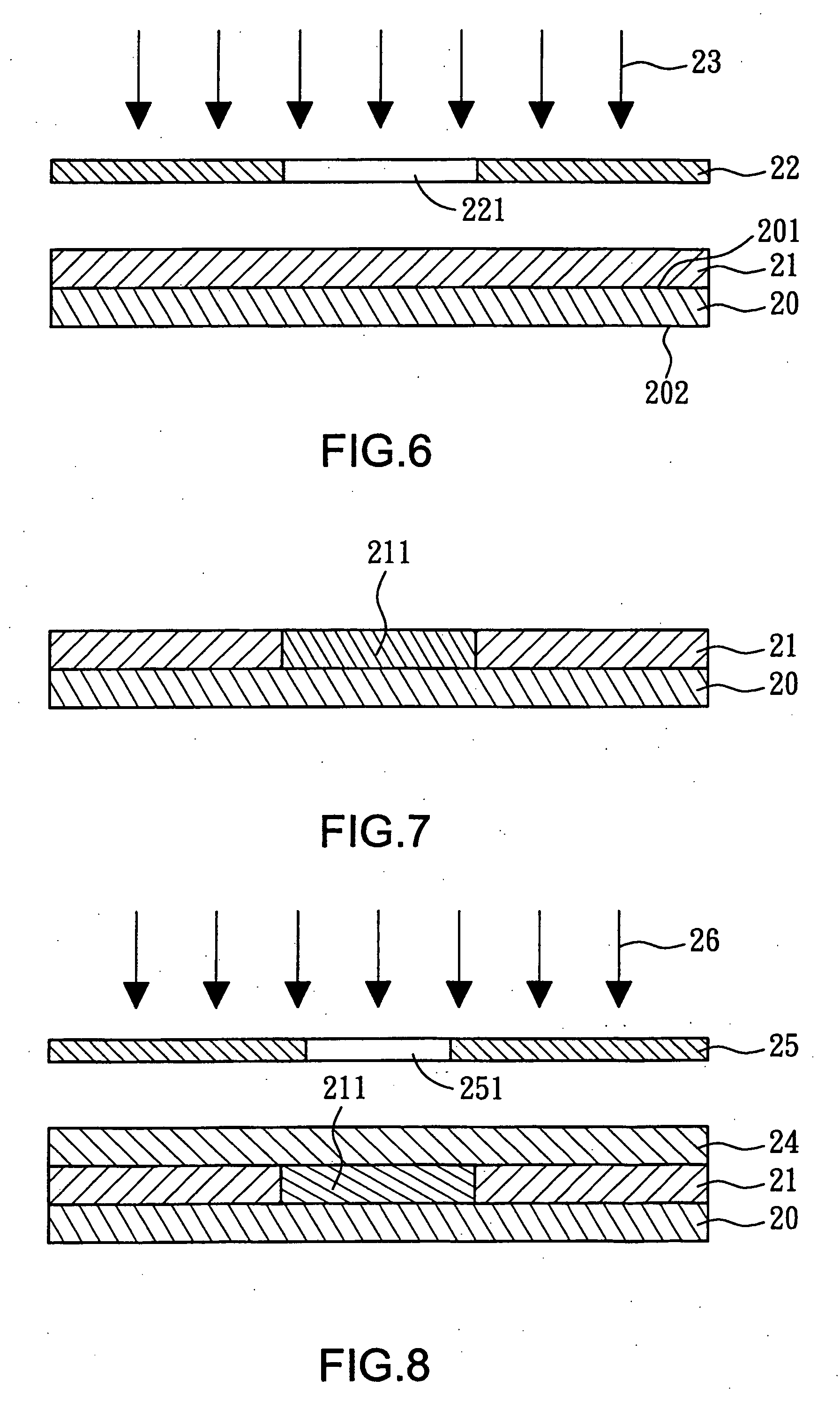
[0032] Referring to FIGS. 6 to 11, schematic views of the method for making a multi-layer photoresist according to the present invention are shown. The method of making the multi-layer photoresist of the present invention comprises the following steps.

[0033] First, referring to FIG. 6, a substrate 20 (e.g., a micro-accelerometer of an optical waveguide element) is provided, and the substrate 20 has an upper surface 201 and a lower surface 202. Next, a first photoresist layer 21 is formed (e.g., coated) on the upper surface 201 of the substrate 20. Then, an exposure procedure is performed on the first photoresist layer 21, such that the first photoresist layer 21 has a first photoreceptive area 211, as shown in FIG. 7.

[0034] In this embodiment, the exposure procedure is described as follows. Referring to FIG. 6 again, firstly, a first mask 22 having a first mask pattern 221 is provided. Next, a first light beam 23 is provided, the first light beam 23 goes through the first mask pat...


PUM

PropertyMeasurementUnit
aspect ratioaaaaaaaaaa
areaaaaaaaaaaa
shapeaaaaaaaaaa

Abstract

The present invention relates to a multi-layer photoresist and the method for making the same and method for etching a substrate. The multi-layer photoresist comprises a plurality of photoresist layers, wherein the photoresist layers have different photoreceptive areas. Therefore, the multi-layer photoresist itself has different light transmitting effects. Thus, a substrate is etched to form a 3D structure by utilizing the multi-layer photoresist directly. The conventional process of applying the photoresist for a second time is not necessary, and naturally the disadvantage that the conventional second photoresist layer is not easily controlled is eliminated, thus the etching quality is improved and the efficiency is high.

Description

BACKGROUND OF THE INVENTION [0001] 1. Field of the Invention [0002] The present invention relates to a photoresist and the method for making the same, and more particularly, to a multi-layer photoresist laminated by a plurality of photoresist layers having different photoreceptive areas and the method for making the same, and a method for etching a substrate is etched to form a recess with a 3D structure by using the multi-layer photoresist. [0003] 2. Description of the Related Art [0004] Referring to FIG. 1, a schematic sectional view of a conventional substrate is shown. The substrate 10 is, for example, a micro-accelerometer of an optical waveguide element, and it has a recess 11 with a 3D structure. As shown in the figure, the recess 11 has a first space 111 and a second space 112. The second space 112 is located under the first space 111, and the width of the first space 111 is larger than that of the second space 112. [0005] Referring to FIGS. 2 to 5, a conventional method for...

Claims


Application Information

Patent Timeline
Patent Type & Authority Applications(United States)
IPC IPC(8): G03C5/00
CPCG03F7/0037G03F7/095
Inventor LIN, JUNG-HONG
Owner CHI LIN TECH CO LTD
Why Eureka
Try Eureka