Supercharge Your Innovation With Domain-Expert AI Agents!

Quantum wells for light conversion

Active Publication Date: 2007-03-01
CREELED INC
View PDF19 Cites 42 Cited by
  • Summary
  • Abstract
  • Description
  • Claims
  • Application Information

AI Technical Summary

Problems solved by technology

One disadvantage of conventional LEDs is that they cannot generate white light from their active layers.
One disadvantage of this approach is that it requires the use of multiple LEDs to produce a single color of light, increasing costs.
In addition, different colors of light are often generated from different types of LEDs which can require complex fabrication to combine in one device.
The resulting devices can also require complicated control electronics since the different diode types can require different control voltages.
Long term wavelength and stability of these devices is also degraded by the different aging behavior of the different LEDs.
In applications such as displays or television screens, this can also result in a prohibitive number of LEDs and can require complex control electronics.
The addition of the phosphor can result in a complex LED that requires a complex manufacturing process.
In addition, the net light emitting efficiency is reduced due to the absorption in the phosphor and the Stokes shift from blue to yellow.
However, conventional blue LEDs operate from a relatively low supply of current that results in a light that can be too dim for many lighting applications.
This problem is compounded by the absorption of some of the blue light by the downconverting material used in generating white light from a blue source.
At this current, LEDs become very hot and any material surrounding the LED will also become hot.
The heat can damage the downconverting material surrounding the LED, degrading its ability to downconvert the LED's light.
The heat can also present a danger of burning objects that are near or in contact with the LED.

Method used


Image

  • Quantum wells for light conversion
  • Quantum wells for light conversion
  • Quantum wells for light conversion

Examples


Embodiment Construction

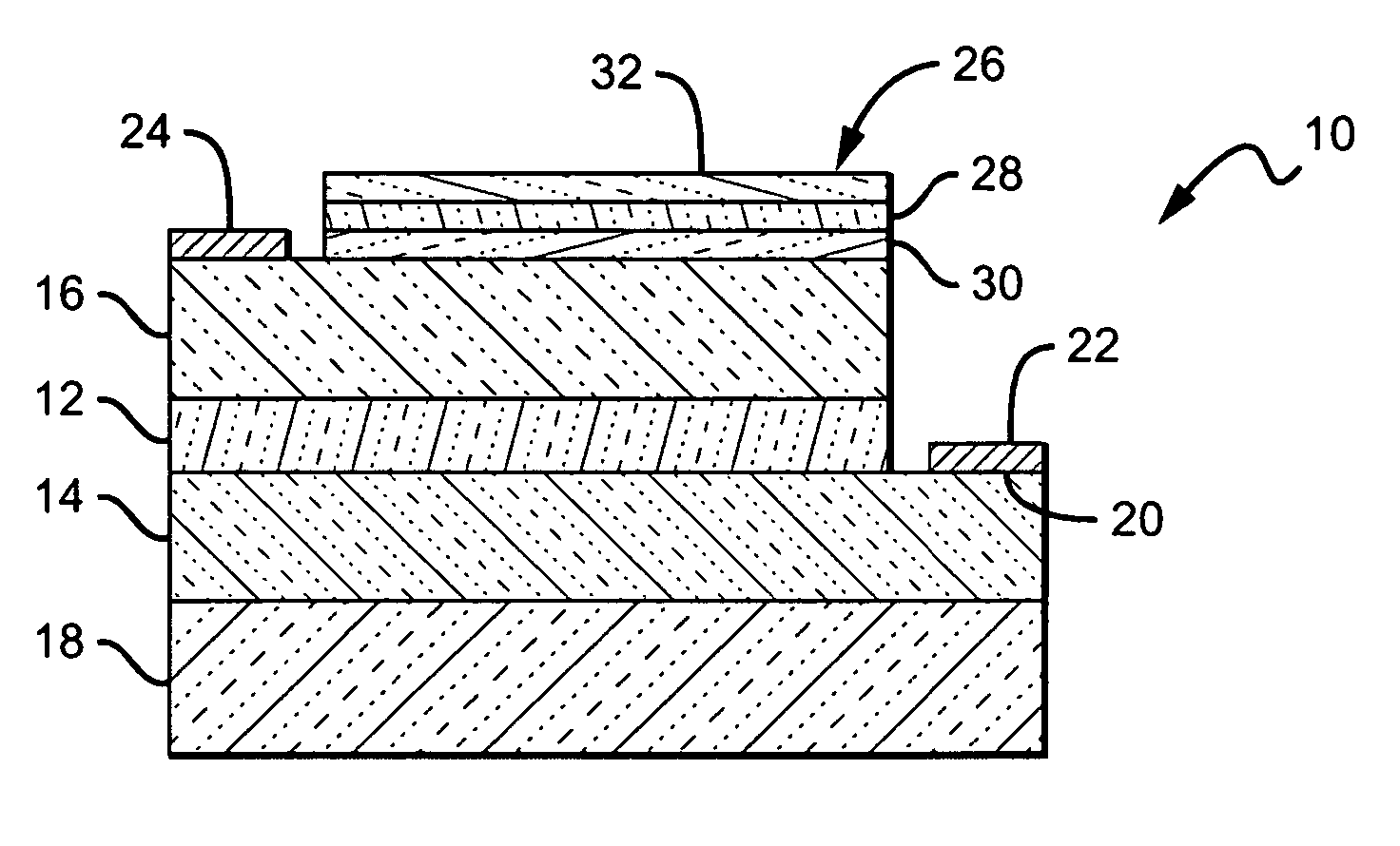
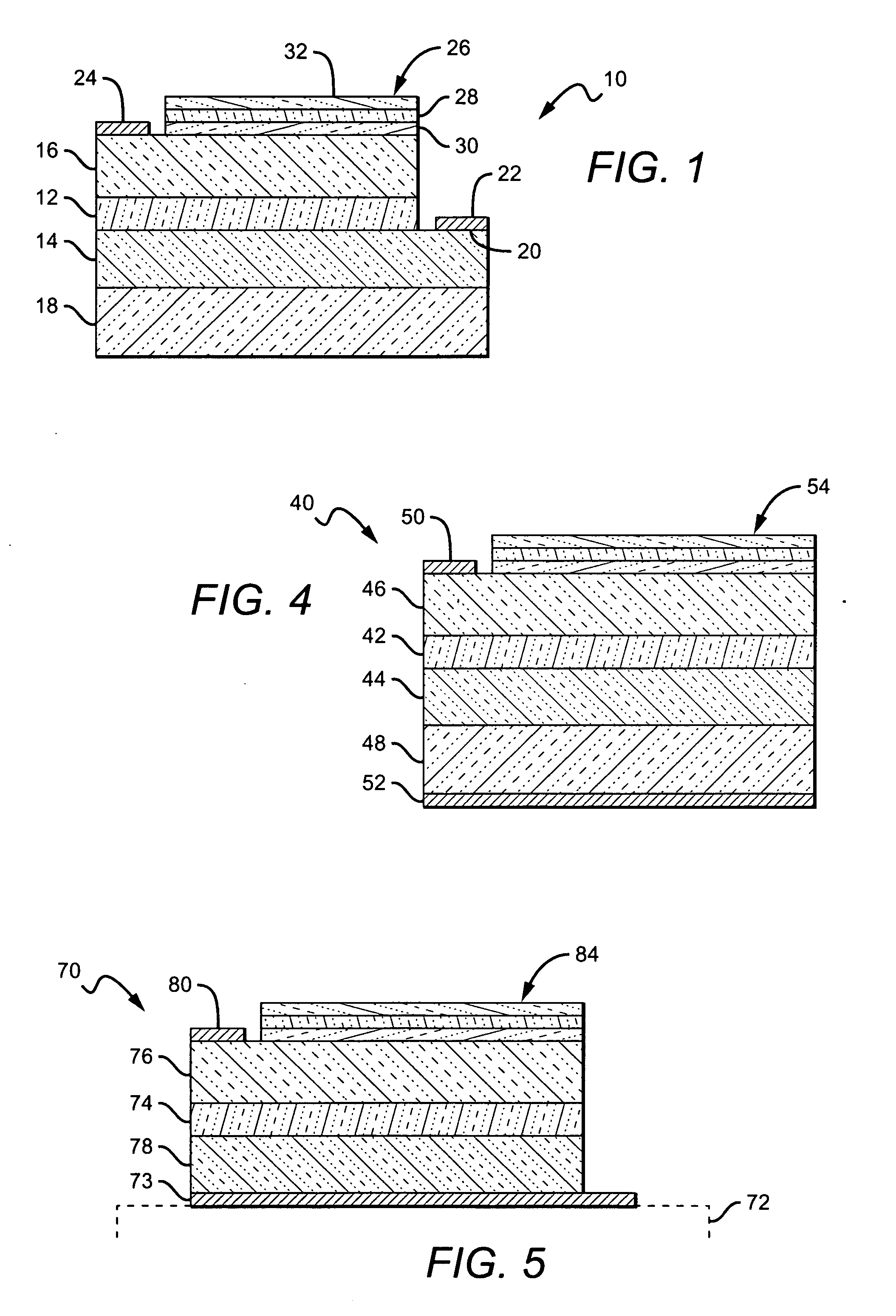
[0025] The present invention is directed to solid state emitters (and methods for light emission) utilizing quantum well structures to absorb light from the active region of the emitters, and re-emit light at a wavelength different from the active region wavelength of light. In one embodiment, the solid state emitter can emit a wavelength combination of light from the active region and the quantum well structures. In other embodiments, the solid state emitter and quantum well structures can be arranged so that the light emitted from the emitter is primarily re-emitted light from the quantum well structure.

[0026] The quantum well structures can be located in many different places integral to the emitters, such as on or within the solid state emitters, with one embodiment having a quantum well structure on an outside surface of the emitter. This allows for the quantum well structure to be formed on the emitter following fabrication (and annealing where necessary) of the emitter layer...


PUM


Abstract

A solid state light emitting device according to the present invention comprises an emitter structure having an active region of semiconductor material and a pair of oppositely doped layers of semiconductor material on opposite sides of said active region. The active region emits light at a first wavelength in response to an electrical bias across said doped layers. A quantum well structure is included that is integral to the emitter structure and has a plurality of layers having a composition and thickness such that the quantum well structure absorbs at least some of the light emitted from the active region and re-emits light of at least one different wavelength of light from said first wavelength.

Description

BACKGROUND OF THE INVENTION [0001] 1. Field of the Invention [0002] This invention relates to solid state light emitting diodes (LEDs) and lasers that can emit various colors of light, including white. [0003] 2. Description of the Related Art [0004] Light emitting diodes (LEDs) are a known class of solid state devices that convert electric energy to light. They generally comprise one or more active layers of semiconductor material sandwiched between oppositely doped layers. When a bias is applied across the doped layers, holes and electrons are injected into the active layer where they recombine to generate light. Light is emitted omnidirectionally from the active layer and from all surfaces of the LED. The useful light is generally emitted in the direction of the LED's top surface, which is usually p-type. [0005] One disadvantage of conventional LEDs is that they cannot generate white light from their active layers. One way to produce white light from conventional LEDs is to combin...

Claims


Application Information

Patent Timeline
IPC IPC(8): H01L31/00
CPCH04L63/0272H04W12/02H04L63/08H04L63/061H01L33/08
Inventor SAXLER, ADAM
Owner CREELED INC
Features
  • R&D
  • Intellectual Property
  • Life Sciences
  • Materials
  • Tech Scout
  • Unparalleled Data Quality
  • Higher Quality Content
  • 60% Fewer Hallucinations
Learn More