Conductive through via structure and process for electronic device carriers

a technology of electronic device carrier and via, which is applied in the direction of coupling device connection, semiconductor/solid-state device details, semiconductor devices, etc., can solve the problems of difficult to completely cover the walls of the bottom level of the via with oxide, difficult to achieve reliable conductive, and difficult to completely fill the via in silicon carrier without leaving voids, etc., to achieve the effect of improving the electronic structure and method of fabricating

Active Publication Date: 2007-03-01
IBM CORP
View PDF13 Cites 203 Cited by
  • Summary
  • Abstract
  • Description
  • Claims
  • Application Information

AI Technical Summary

Benefits of technology

[0012] It is an object of the present invention to provide ...

Problems solved by technology

One of the difficulties with fabricating conductive vias in carriers, such as silicon, is forming vias that are reliable.
In this regard, a number of processing factors and limitations act to create difficulties in achieving reliable conductive through vias.
There are, however, a number of difficulties with this type of approach.
One difficulty is that this approach requires that the insulation and subsequent metallization must typically completely fill each via, if any wiring layers are to be added to the top.
In addition, completely filling vias in silicon carriers without leaving voids is problematic, particularly in deep vias.
On the other hand, where passivation is accomplished by chemical vapor deposition (CVD) after BEOL processing, it is difficult to completely cover the walls with oxide in the lower levels of deep vias, particularly around the region of generally intersecting vertical and bottom surfaces, since CVD is not fully con...

Method used


Image

  • Conductive through via structure and process for electronic device carriers
  • Conductive through via structure and process for electronic device carriers
  • Conductive through via structure and process for electronic device carriers

Examples


Embodiment Construction

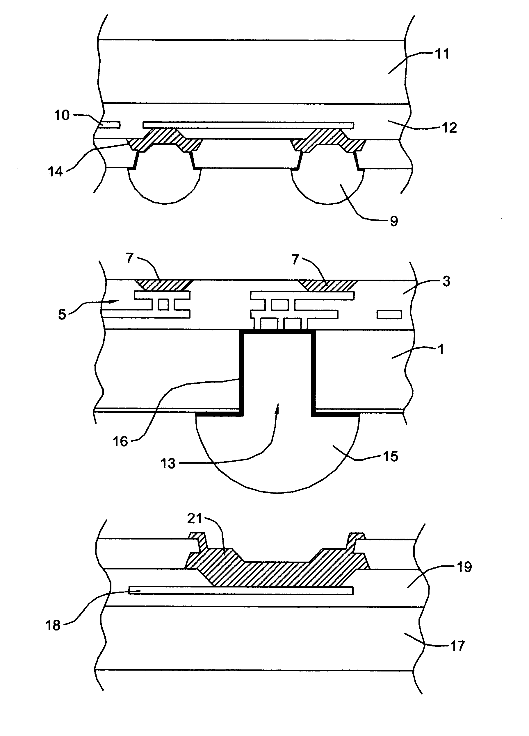
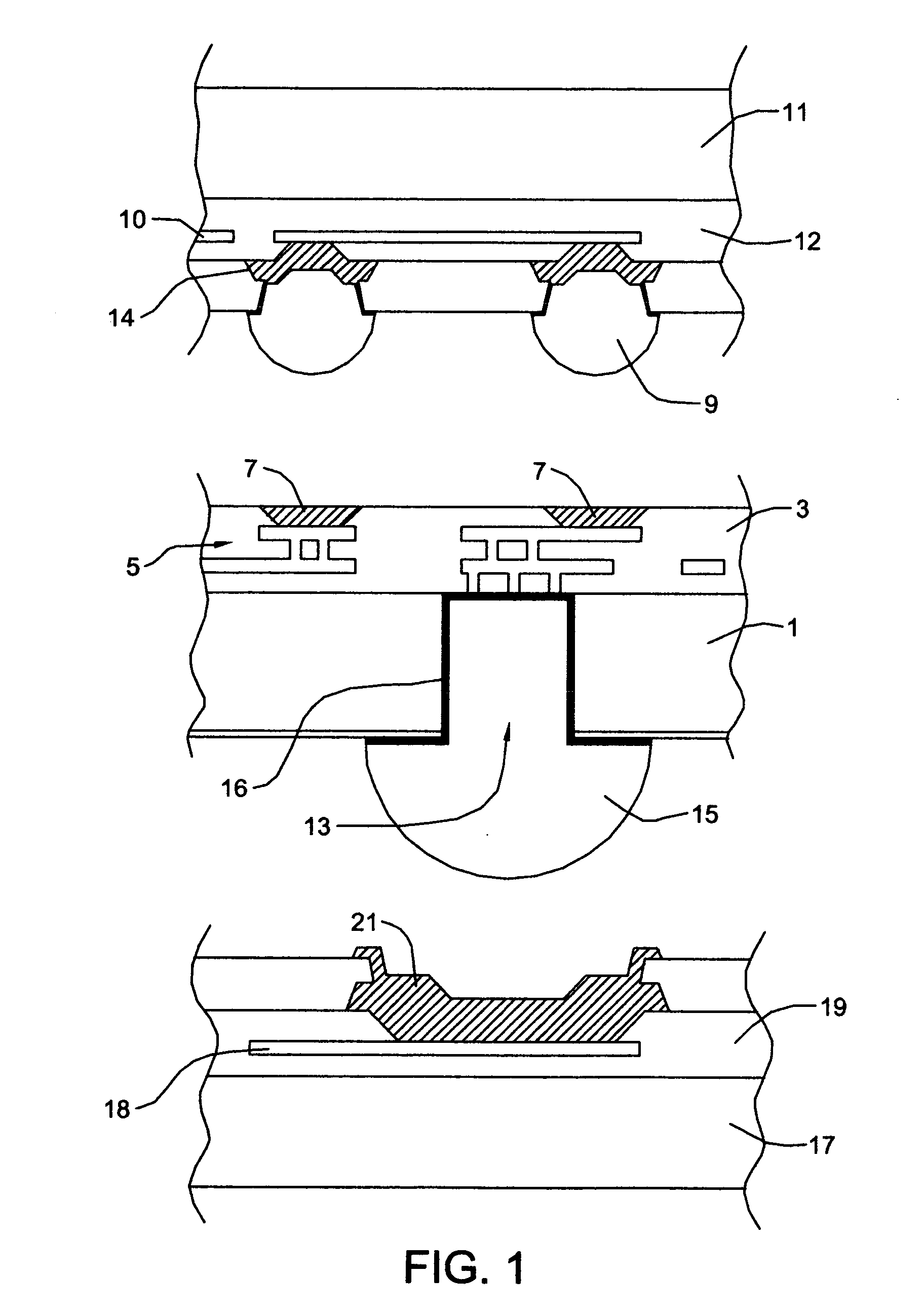
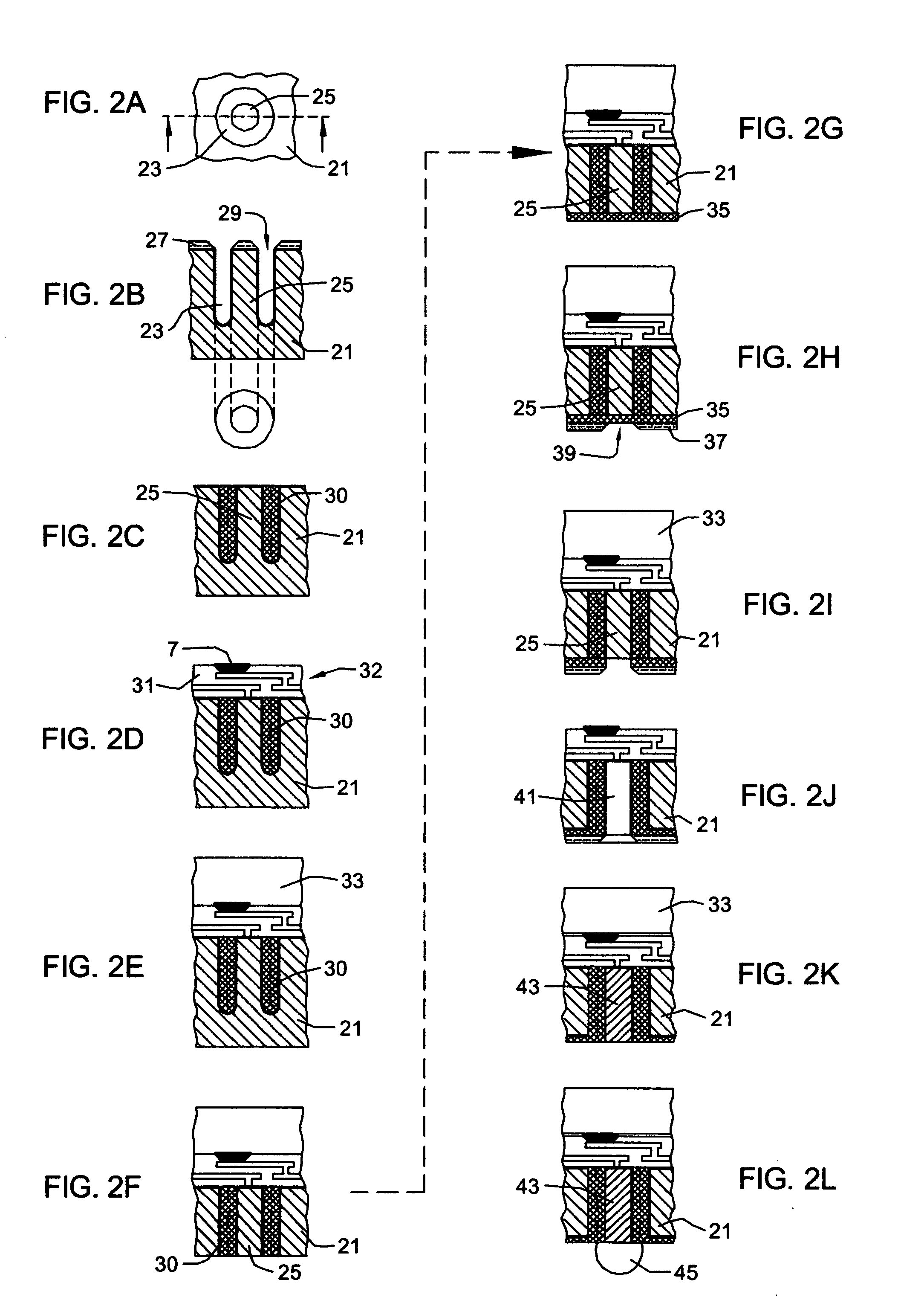
[0040] In accordance with the present invention, conductive through vias in electronic device structures, such as, wafer, chips components and the like and in electronic device carriers for same are provided by forming an annulus or ring cavity in the carrier and forming insulating material in the cavity. The carrier material circumscribed by the insulating material is replaced by conductive material to form a conductive through via.

[0041] The process allows for the formation of an annular insulating region that surrounds and isolates the conductive via and that is formed independent of the creation of the conductive via. The process effectively allows the via passivation step to be carried out independent of the via conductive fill step. In addition, since the annulus cavity structure requires far less material to be removed than conventional open cylinder approaches and presents twice the wall surface area on which to form insulation and deposit metal, small annulus gaps may be c...


PUM

PropertyMeasurementUnit
Electrical conductivityaaaaaaaaaa
Volumeaaaaaaaaaa
Electrical conductoraaaaaaaaaa

Abstract

Conductive through vias are formed in electronic devices and electronic device carrier, such as, a silicon chip carrier. An annulus cavity is etched into the silicon carrier from the top side of the carrier and the cavity is filled with insulating material to form an isolation collar around a silicon core region. An insulating layer with at least one wiring level, having a portion in contact with the silicon core region, is formed on the top side of the carrier. Silicon is removed from the back side of the carrier sufficient to expose the distal portion of the isolation collar. The core region is etched out to expose the portion of the wiring level in contact with the silicon core region to form an empty via. The via is filled with conductive material in contact with the exposed portion of the wiring level to form a conductive through via to the wiring level. A solder bump formed, for example, from low melt C4 solder, is formed on the conductive via exposed on the carrier back side. The process acts to make the conductive via fill step independent of the via isolation step.

Description

[0001] This invention was made with Government support under Contract NBCH30390004 awarded by the Defense Advanced Research Projects Agency and under Contract H98230-04-C-0920 awarded by the Maryland Procurement Office. The government has certain rights in this invention.BACKGROUND OF THE INVENTION [0002] 1. Field of the Invention [0003] The present invention relates to electrically interconnecting via structures and methods of making same in material, such as, semiconductor material. More particularly, the present invention relates to conductive through via structures and processes for making same in electronic device structures, such as in semiconductor wafers, chips, components and the like, and in electronic device carriers for such semiconductor wafers, chips, components and the like. [0004] 2. Background and Related Art [0005] In the packaging of electronic devices, such as, semiconductor chips or wafers, device carriers are used to interconnect the devices. Where electronic d...

Claims


Application Information

Patent Timeline
IPC IPC(8): H01L21/00H01R12/71
CPCH01L21/4853H01L21/486H01L2924/0002Y10T29/49165H01L2224/0401H01L21/6835H01L21/76898H01L23/481H01L23/49816H01L23/49827H01L23/49833H01L2924/09701H01L2924/12044H01L2924/3011H01L2224/16225H01L2224/05567H01L2224/13009H01L2224/13022H01L2221/68345H01L2224/131H01L2224/16227H01L2224/81191H01L2924/014H01L2224/05552
Inventor ANDRY, PAUL S.PATEL, CHIRAG S.SPROGIS, EDMUND J.TSANG, CORNELIA K.
Owner IBM CORP
Why Eureka
Try Eureka