Semiconductor memory device with dielectric structure and method for fabricating the same

a memory device and semiconductor technology, applied in the direction of semiconductor devices, electrical appliances, transistors, etc., can solve the problems of difficult formation of dielectric layers, limitation of increasing dielectric constant, capacitor size cannot be reduced in proportion to memory cell region reduction, etc., to improve leakage current characteristics.

Inactive Publication Date: 2007-03-08
SK HYNIX INC
View PDF31 Cites 43 Cited by
  • Summary
  • Abstract
  • Description
  • Claims
  • Application Information

AI Technical Summary

Benefits of technology

[0008] It is, therefore, an object of the present invention to provide a dielectric layer capable of securing a dielectric capacity and improving a leakage current characteristic, and a method for fabricating the same.

Problems solved by technology

However, the size of a capacitor cannot be reduced in proportion to the memory cell region reduction.
Even if the thickness of the dielectric layer is reduced or the surface region of the dielectric layer is enlarged, there still exists a limitation in increasing the dielectric constant.
Thus, it is difficult to form a dielectric layer using SiON or Al2O3 in a thickness of approximately 40 Å or below.
However, if the SrTiO3 layer is formed in a thickness of approximately 100 Å or under, the dielectric constant and the leakage current characteristic are rapidly deteriorated.
Although a HfO2 layer has a high dielectric constant of 25, it may be difficult to apply the HfO2 layer solely because the HfO2 layer has a heat stability limitation due to a low crystallization temperature, resulting in high leakage current.
However, such structure generates a dielectric capacity loss due to the low dielectric constant (ε) of Al2O3, (i.e., ε=9).

Method used


Image

  • Semiconductor memory device with dielectric structure and method for fabricating the same
  • Semiconductor memory device with dielectric structure and method for fabricating the same
  • Semiconductor memory device with dielectric structure and method for fabricating the same

Examples


first embodiment

[0026] Hereinafter, the present invention will be described in detail.

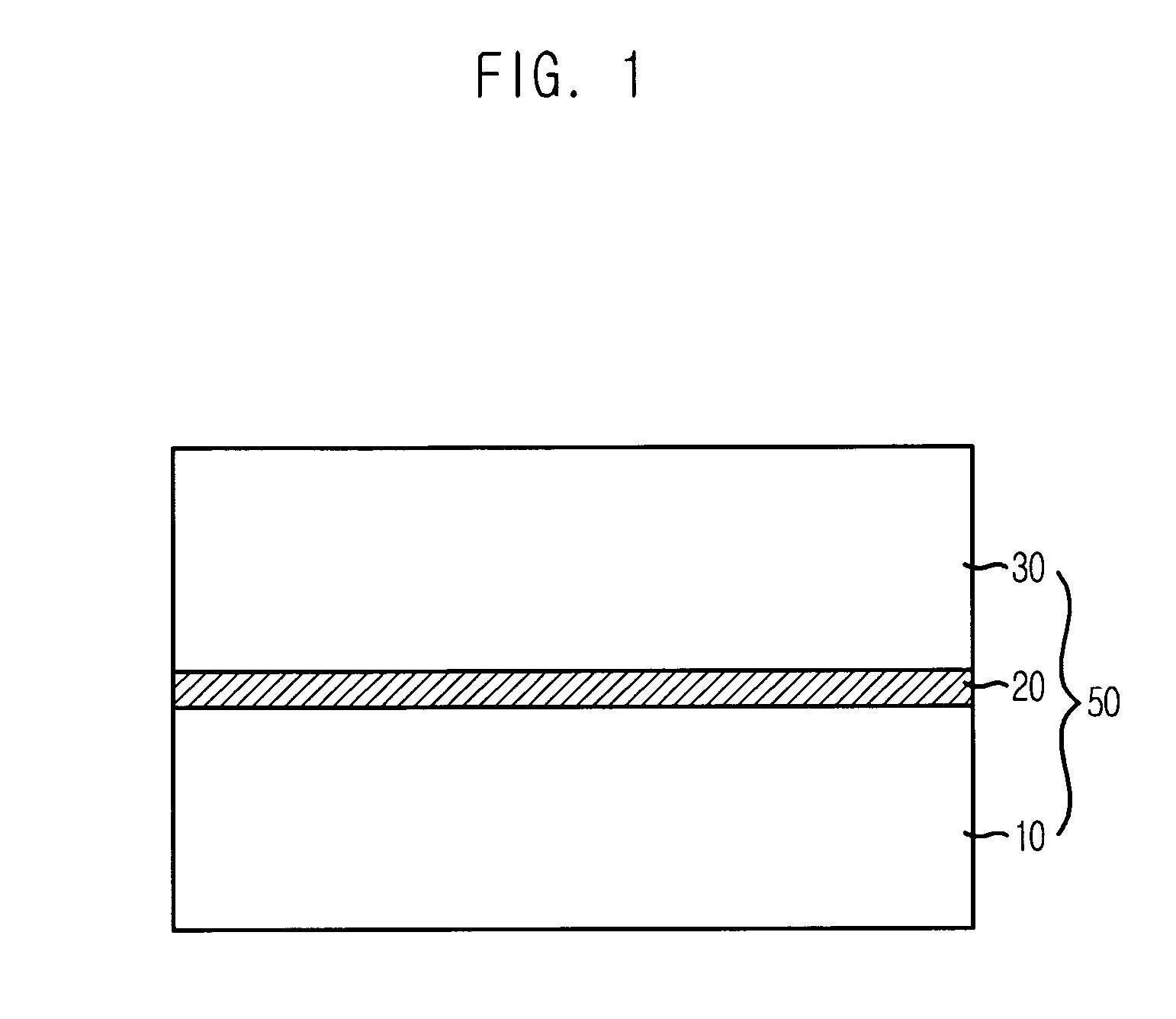
[0027]FIG. 1 is a cross-sectional view illustrating a dielectric structure in accordance with the first embodiment of the present invention.

[0028] As shown in FIG. 1, a dielectric structure 50 includes: a first dielectric layer 10 having a dielectric constant of 25 or higher; a second dielectric layer 20 including a material having a crystallization rate lower than the first dielectric layer 10; and a third dielectric layer 30 including a material substantially identical to the first dielectric layer 10. Herein, the second dielectric layer 20 is formed on the first dielectric layer 10, and the third dielectric layer 30 is formed on the second dielectric layer 20. Herein, the crystallization rate refers to the probability of a layer to become crystallized by various external factors including temperature. Preferably, the crystallization rate described in the specific embodiments of the present invention refers to ...

second embodiment

[0051] Hereinafter, the present invention is described in detail.

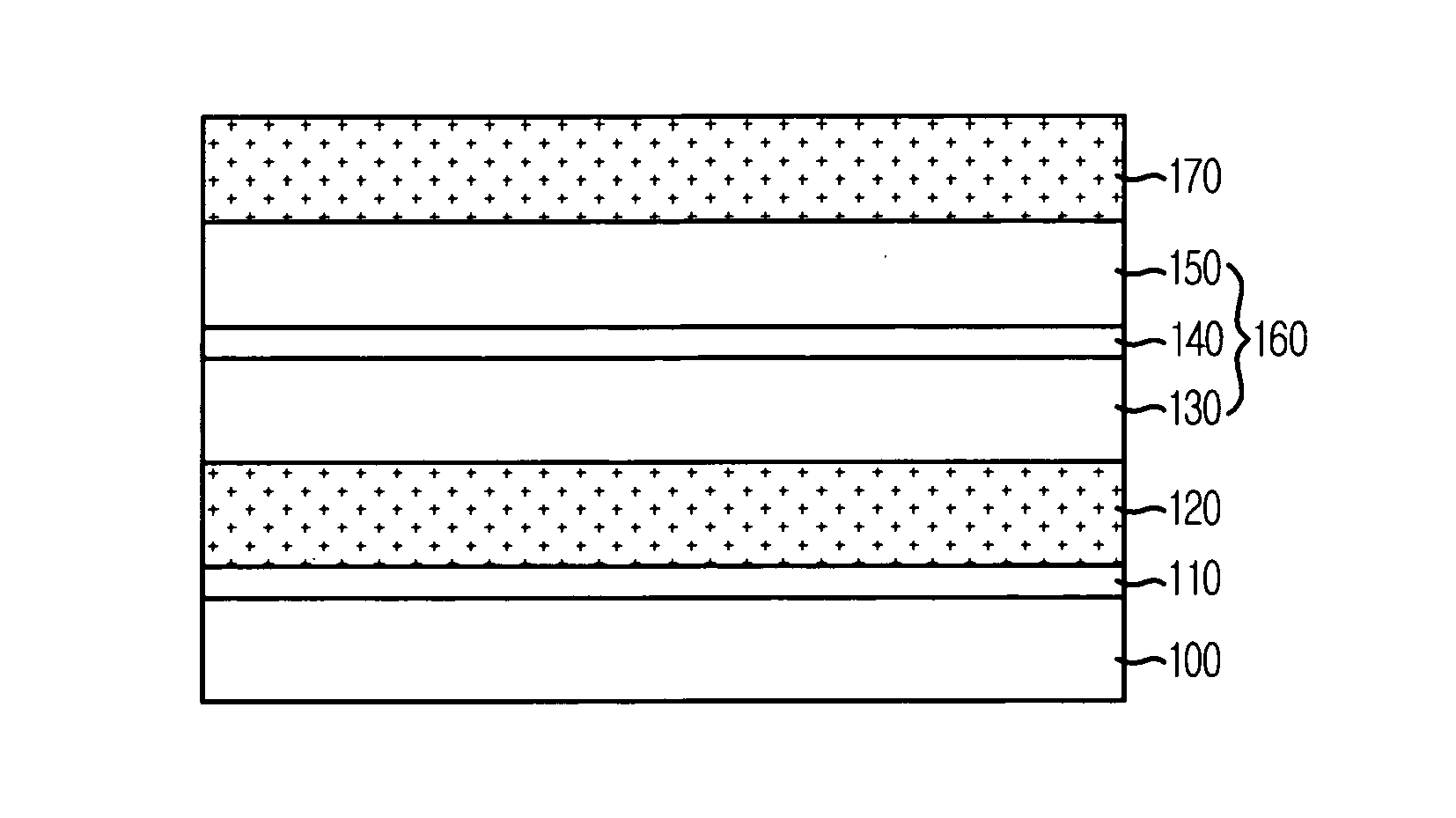
[0052] The dielectric structure in accordance with the first embodiment of the present invention can be generally applied in a capacitor of a dynamic random access memory (DRAM). FIG. 7 is a cross-sectional view illustrating a capacitor formed in accordance with the second embodiment of the present invention, wherein the second embodiment is an example whereto the first embodiment of the present invention is applied. Herein, a stack type capacitor is illustrated for the convenience of description. However, the stack type capacitor is one of many examples of application. The first embodiment of the present invention can be applied to a concave type or a cylinder type capacitor.

[0053] Referring to FIG. 7, the capacitor in accordance with the second embodiment of the present invention includes: a substrate 100 on which predetermined processes including transistor and bit lines formation are completed; an inter-layer diel...

third embodiment

[0064] Hereinafter, the present invention is described in detail.

[0065] A dielectric layer in accordance with the first embodiment of the present invention can be applied to an inter-poly dielectric (IPD) structure or an inter-poly oxide (IPO) structure in a non-volatile memory device. FIG. 8 is a cross-sectional view illustrating a non-volatile memory device formed in accordance with the third embodiment of the present invention, wherein the third embodiment is an example whereto the first embodiment of the present invention is applied.

[0066] The non-volatile memory device includes: a substrate 200 whereon a gate insulation layer 210 is formed; a floating gate 220 formed over a predetermined portion of the gate insulation layer 210; a dielectric structure 260 formed in accordance with the first embodiment of the present invention; and a control gate 270 formed over the dielectric structure 260. Herein, the dielectric structure 260 has a configuration substantially identical to tha...


PUM

PropertyMeasurementUnit
dielectric constantaaaaaaaaaa
temperatureaaaaaaaaaa

Abstract

A semiconductor memory device with a dielectric structure and a method for fabricating the same are provided. The dielectric structure includes: a first dielectric layer having a dielectric constant of approximately 25 or higher; a second dielectric layer including a material having a crystallization rate lower than the first dielectric layer and formed over the first dielectric layer; and a third dielectric layer including a material substantially identical to that of the first dielectric layer and formed over the second dielectric layer.

Description

FIELD OF THE INVENTION [0001] The present invention relates to a semiconductor memory device and a method for fabricating the same; and, more particularly, to a semiconductor memory device provided with a dielectric layer and a method for fabricating the same. DESCRIPTION OF RELATED ARTS [0002] For a semiconductor memory device, e.g., a DRAM device, the size of a memory cell region for storing 1 bit has become smaller as the degree of integration has increased. Herein, 1 bit is the basic unit for memory information. However, the size of a capacitor cannot be reduced in proportion to the memory cell region reduction. This result is because a dielectric capacity above a certain level is required for each of the unit cells to prevent soft errors and maintain stable operations. Thus, researches for maintaining the capacity of the capacitor within the limited cell region above a certain level are being demanded. Such researches have progressed in three different ways. The first one is a ...

Claims


Application Information

Patent Timeline
Patent Type & Authority Applications(United States)
IPC IPC(8): H01L29/94
CPCH01L21/28273H01L29/7881H01L29/513H01L29/40114H10B12/00
Inventor KIL, DEOK-SINHONG, KWONYEOM, SEUNG-JIN
Owner SK HYNIX INC
Why Eureka
Try Eureka