Non-Volatile Memory Devices Having L-Shaped Floating Gate Electrodes and Methods of Forming Same

a floating gate electrode and non-volatile technology, applied in semiconductor devices, digital storage, instruments, etc., can solve the problems of increasing reducing changing the threshold voltage of the eeprom cell, so as to reduce the parasitic cell-to-cell coupling capacitance, reduce the coupling ratio, and reduce the coupling capacitance of the cell-to-cell.

Inactive Publication Date: 2007-03-08
SAMSUNG ELECTRONICS CO LTD
View PDF5 Cites 23 Cited by
  • Summary
  • Abstract
  • Description
  • Claims
  • Application Information

AI Technical Summary

Benefits of technology

[0009] Embodiments of the invention include non-volatile memory devices having memory cells therein with reduced cell-to-cell coupling capacitance. According to some of these embodiments, non-volatile memory devices, such as NAND-type flash EEPROM devices, include memory cells with floating gate electrodes. These floating gate electrodes are formed to have an open-ended wraparound shape that operates to reduce parasitic cell-to-cell coupling capacitance in a bit line direction while maintaining a high coupling ratio between control and floating gate electrodes within each memory cell. In particular, each memory cell may include an EEPROM transistor therein. Each of these EEPROM transistors includes a tunneling insulating layer on a semiconductor channel region and a floating gate electrode on the tunneling insulating layer. The floating gate electrode has an open-ended wraparound shape that is filled with an electrically insulating region. According to some of these embodiments, the floating gate electrode may be shaped as a rectangular cylinder with a hollow center that is filled with the electrically insulating region.

Problems solved by technology

These operations to attract electrons to the floating gate electrode or withdraw electrons from the floating gate electrode result in a change in a threshold voltage of the EEPROM cell.
In particular, operations to program an EEPROM cell may result in an increase in the threshold voltage of the EEPROM cell and operations to erase an EEPROM cell may result in a decrease in the threshold voltage of the EEPROM cell, as described above for both single and multi-level cells.
Unfortunately, as EEPROM devices become more highly integrated on a semiconductor substrate, the parasitic capacitance between floating gate electrodes of closely adjacent EEPROM cells may increase.
These increases in parasitic capacitance caused by higher device integration levels can result in a corresponding increase in floating gate interference.
If this interference is sufficiently high, then the programming of one EEPROM cell may result in a threshold voltage shift of one or more closely adjacent EEPROM cells in the neighborhood of the EEPROM cell undergoing programming.
Such shifts in threshold voltage can reduce memory device reliability by causing bit errors to occur during data reading operations.

Method used


Image

  • Non-Volatile Memory Devices Having L-Shaped Floating Gate Electrodes and Methods of Forming Same
  • Non-Volatile Memory Devices Having L-Shaped Floating Gate Electrodes and Methods of Forming Same
  • Non-Volatile Memory Devices Having L-Shaped Floating Gate Electrodes and Methods of Forming Same

Examples


Embodiment Construction

[0038] The present invention now will be described more fully herein with reference to the accompanying drawings, in which preferred embodiments of the invention are shown. This invention may, however, be embodied in many different forms and should not be construed as being limited to the embodiments set forth herein; rather, these embodiments are provided so that this disclosure will be thorough and complete, and will fully convey the scope of the invention to those skilled in the art. Like reference numerals refer to like elements throughout and signal lines and signals thereon may be referred to by the same reference characters.

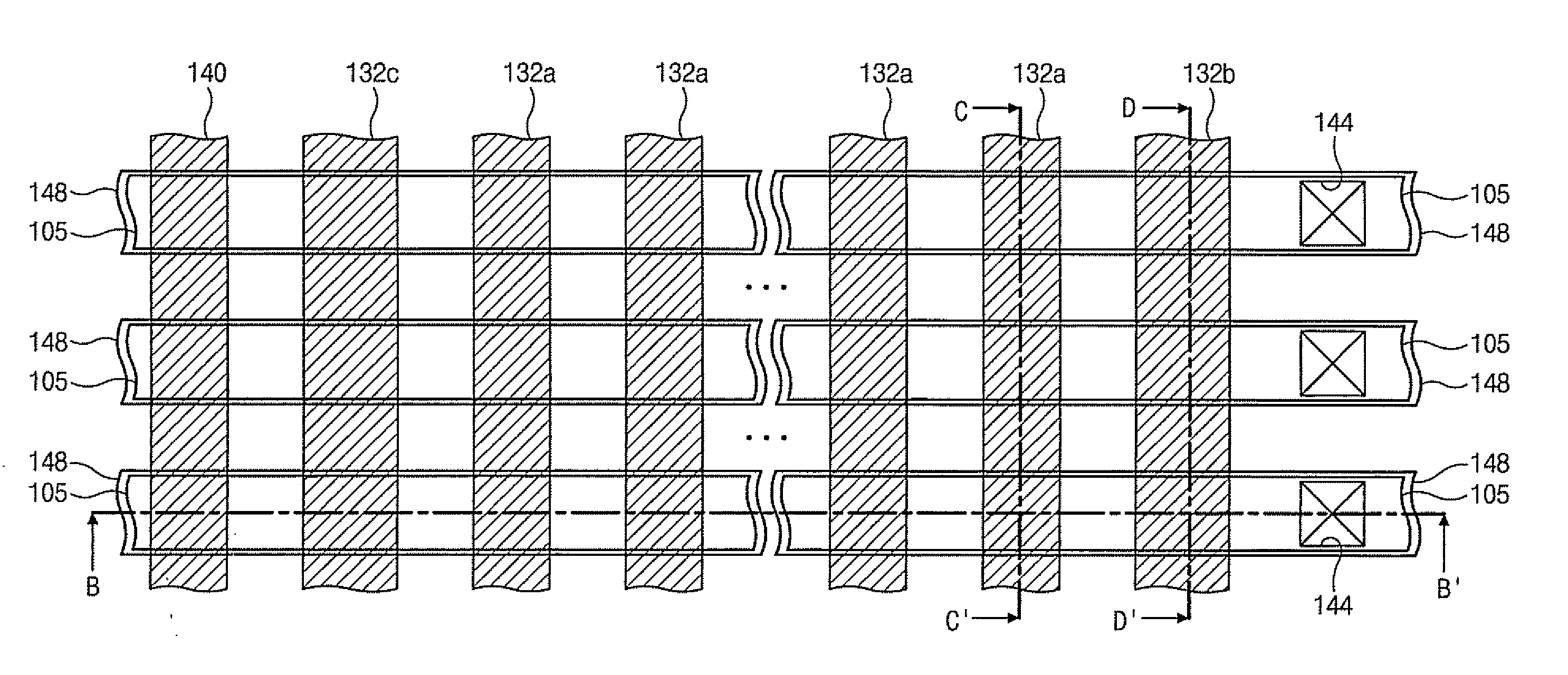
[0039] A NAND-type EEPROM device according to first embodiments of the invention is illustrated by FIGS. 2A-2D. In particular, FIG. 2A, which is a plan layout view of a NAND-type EEPROM device, illustrates a plurality of bit lines 148 that extend in parallel in a first direction across a semiconductor substrate 100 having active regions 105 therein. As sh...


PUM


Abstract

A flash EEPROM array includes a first row of EEPROM cells having a first floating gate electrode therein and a second row of EEPROM cells having a second floating gate electrode therein. The first floating gate electrode includes at least one horizontal segment and at least one vertical segment, which collectively define a first L-shaped portion of the first floating gate electrode that faces a first direction. The second floating gate electrode includes at least one horizontal segment and at least one vertical segment that collectively define a second L-shaped portion of the second floating gate electrode that faces a second direction opposite the first direction.

Description

REFERENCE TO PRIORITY APPLICATIONS [0001] This application is a continuation-in-part (CIP) of U.S. application Ser. No. 11 / 464,324, filed Aug. 14, 2006, the disclosure of which is hereby incorporated herein by reference. This application also claims priority to Korean Application Serial No. 2005-0081894, filed Sep. 2, 2005, the disclosure of which also is hereby incorporated herein by reference.FIELD OF THE INVENTION [0002] The present invention relates to integrated circuit memory devices and methods of forming same and, more particularly, to non-volatile memory devices and methods of forming non-volatile memory devices. BACKGROUND OF THE INVENTION [0003] One class of nonvolatile memory devices includes electrically erasable programmable read only memory (EEPROM), which may be used in many applications including embedded applications and mass storage applications. In typical embedded applications, an EEPROM device may be used to provide code storage in personal computers or mobile ...

Claims


Application Information

Patent Timeline
Patent Type & Authority Applications(United States)
IPC IPC(8): G11C11/34
CPCH01L21/28273H01L27/115H01L29/42324H01L27/11524H01L27/11521H01L29/40114H10B41/35H10B69/00H10B41/30H01L21/76838
Inventor CHOI, JEONG HYUK
Owner SAMSUNG ELECTRONICS CO LTD
Why Eureka
Try Eureka