Through-hole forming method, and piezoelectric device manufacturing method and piezoelectric device manufactured thereby

a piezoelectric device and manufacturing method technology, applied in the direction of piezoelectric/electrostrictive transducers, transducer types, printing, etc., can solve the problems of gas or dust ingress into the interior space, the conductivity between the external electrode and the leading electrode cannot be established, and the gap may be created. , to achieve the effect of high conductivity and high air tightness

Inactive Publication Date: 2007-03-15
SEIKO EPSON CORP
View PDF6 Cites 46 Cited by
  • Summary
  • Abstract
  • Description
  • Claims
  • Application Information

AI Technical Summary

Benefits of technology

[0007] An advantage of some aspects of the invention is to resolve the above stated problems and thereby to provide a method of forming the part of a through-hole for piezoelectric substrate which enables to ensure a high airtight sealing to the excitation space and to establish conductivity between the exterior electrodes and the leading electrodes, respectively, within the excitation space with ease, and a method of manufacturing the piezoelectric device using the above method and the piezoelectric device manufactured thereby.

Problems solved by technology

First, since the piezoelectric substrate serving as the covering body is formed on one surface with the concave portion and the part of a through-hole, there is a high possibility for foreign matters to be attached to and remaining at the concave portion and the part of a through-hole while cleaning the substrate or the like.
Second, the piezoelectric substrate and the covering body are bonded through a thin metal film formed around an edge portion of the piezoelectric substrate, such that there is a possibility that a gap may be created between each of the leading electrodes and each of the part of a through-hole.
In this case, there arise possible troubles that conductivity between the external electrodes and the leading electrodes can not be established and an airtight sealing of an interior space may be degraded, thereby inviting a possibility of an undesirable invasion of gas or dust from the gap into the interior space.
Further, the part of a through-hole are thus formed on the piezoelectric substrate on which the excitation electrode and the leading electrodes are formed and the conductive members are thus disposes within the part of a through-hole in a manner direct to and continuously with the leading electrodes made of thin metal films, and therefore, there is only a little fear in occurring bad conductivity due to the gap created between the corresponding part of a through-hole and the leading electrodes.

Method used


Image

  • Through-hole forming method, and piezoelectric device manufacturing method and piezoelectric device manufactured thereby
  • Through-hole forming method, and piezoelectric device manufacturing method and piezoelectric device manufactured thereby
  • Through-hole forming method, and piezoelectric device manufacturing method and piezoelectric device manufactured thereby

Examples


first embodiment

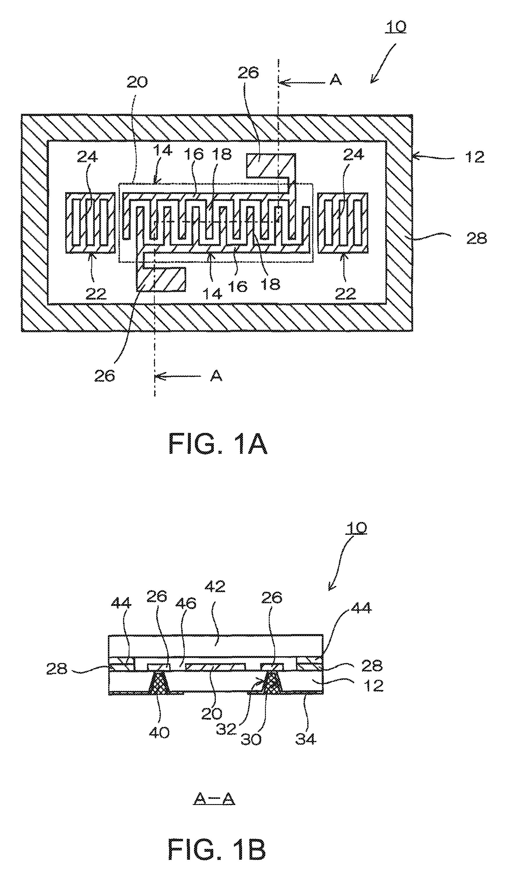
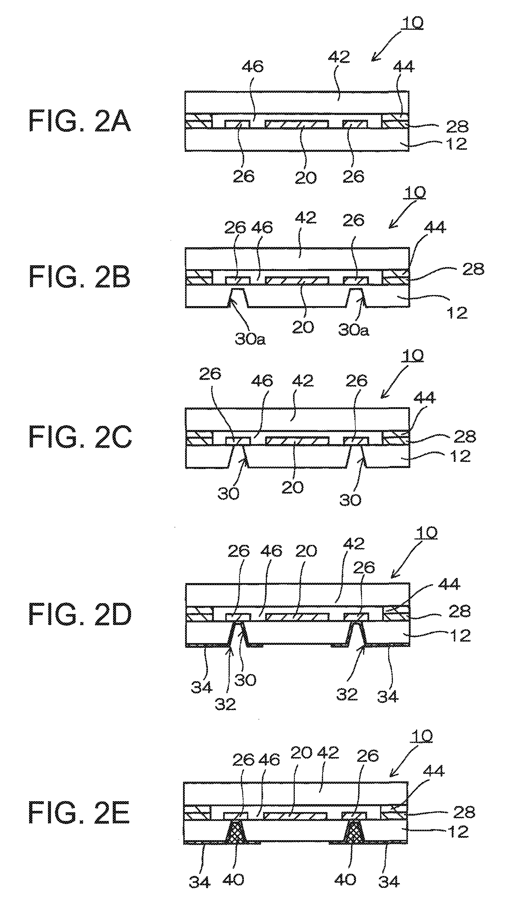
[0029] Explained hereinafter is the piezoelectric device according to the invention, referring to FIG. 1 and exemplifying a SAW element. In FIG. 1, FIG. 1A is a plane view of the SAW element and FIG. 1B is a view taken along a line A-A of the same FIG. 1A. A SAW element 10 of the embodiment includes a piezoelectric substrate 12 and a covering body 42 which covers a first surface of the piezoelectric substrate 12. The piezoelectric substrate 12 is formed with an interdigital transducer (IDT) 20 which is formed such that a pair of comb-shaped electrodes 14, each being composed of bus bars 16 arranged along with a propagation direction of a surface acoustic wave and a plurality of electrode fingers 18 formed orthogonal to the bus bars 16, are placed in a interlocked manner, and a pair of reflectors 22 sandwiching the IDT 20 is placed in the propagation direction of surface acoustic wave. The reflectors 22 are formed into grid-like shapes in which the electrode fingers 18 composing the ...

second embodiment

[0040] the piezoelectric device according to the invention is explained next, referring to FIG. 3. A basic structure of the piezoelectric device according to the second embodiment is similar to that of the piezoelectric device, i.e., the SAW element, according to the first embodiment stated above. Accordingly, components having the same functions as those in the first embodiment will be given the same symbols in drawings and omitted of detailed explanations thereof.

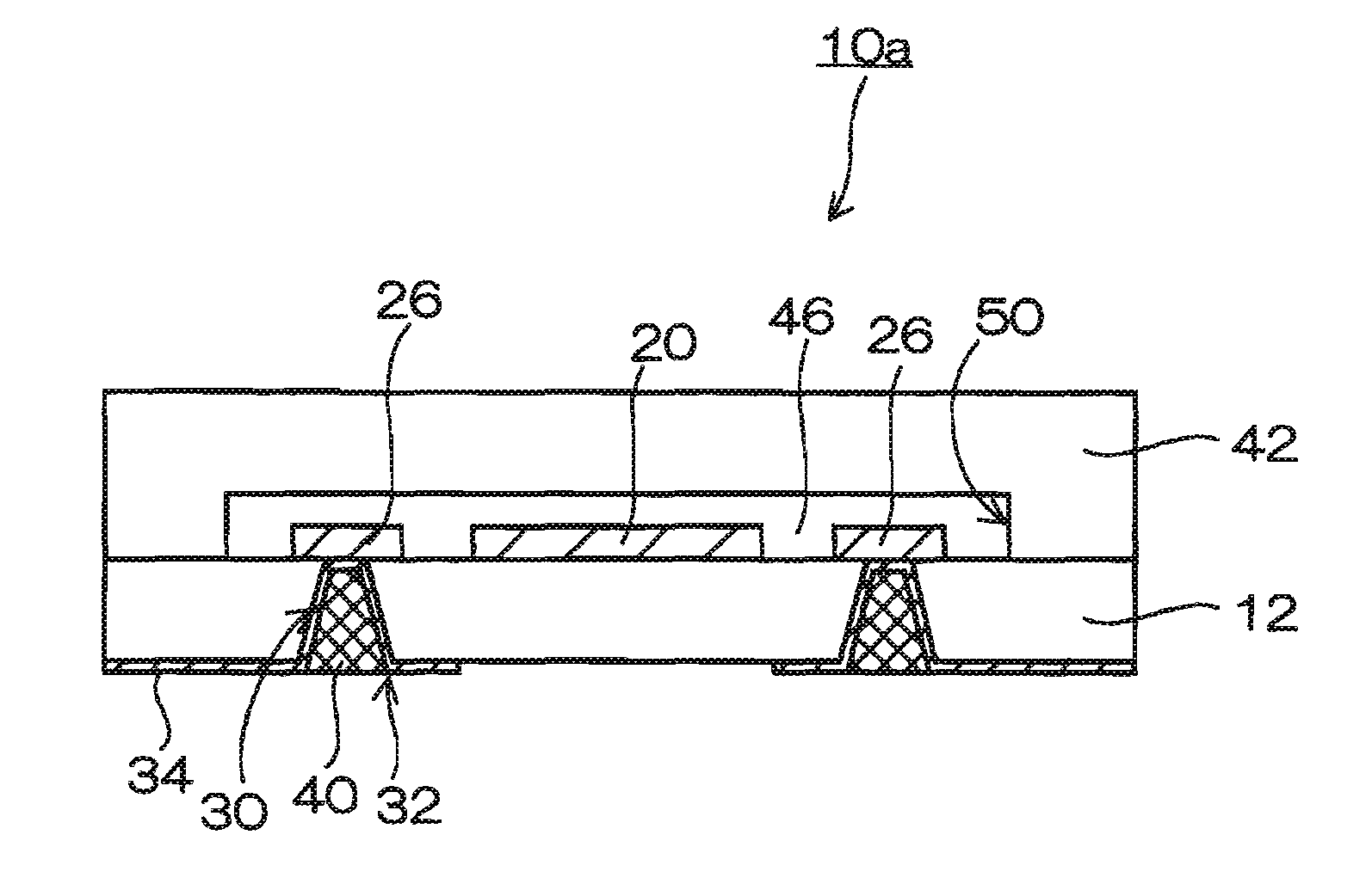
[0041] A SAW element 10a according to the second embodiment is featured in that the bonding method between the piezoelectric substrate 12 and the covering body 42 is different from that of the SAW element 10 according to the first embodiment. More specifically, the SAW element 10a according to the second embodiment employs a direct bonding without using bonding films between bonding surfaces as a method to bond the piezoelectric substrate 12 and the covering body 42.

[0042] The direct bonding is a method to bond the piezo...

third embodiment

[0046] The anodic bonding is a kind of direct bonding. However, unlike the above stated direct bonding, the anodic bonding is a method enabling a direct bonding not only between the crystal surfaces but also between a crystal surface and a glass surface or between metal surfaces and so on by generating a Si—O covalent bonding without requiring bonding films therebetween. In other words, although FIG. 4 shows that the metal pattern 28 formed on the piezoelectric substrate as a bonding section and the covering body 42 are to be bonded, it is also possible to bond the piezoelectric substrate 12 with the covering body 42 without interposing the metal pattern 28 therebetween. More specifically, the piezoelectric substrate 12 and the covering body 42 are placed at a temperature of around several hundreds degrees centigrade and subsequently a direct current of a voltage of several hundreds voltages are applied thereto so as to generate the covalent bonding between the piezoelectric substra...


PUM

PropertyMeasurementUnit
conductivityaaaaaaaaaa
conductiveaaaaaaaaaa
piezoelectricaaaaaaaaaa

Abstract

In a method of forming a part of a through-hole for a piezoelectric substrate having an excitation electrode and a leading electrode which are formed on a first surface of the piezoelectric substrate and are made of a thin metal film in order to establish a conductivity, the method includes: blasting a position on a second surface of the piezoelectric substrate corresponding to the leading electrode to form a preliminary hole by boring the piezoelectric substrate in its halfway; etching a bottom of the preliminary hole to form a part of a through-hole through which a part of the leading electrode is exposed; and placing a conductive material in the part of a through-hole, the conductive material contacting the leading electrode from a side of the second surface of the piezoelectric substrate.

Description

BACKGROUND [0001] 1. Technical Field [0002] The present invention relates to a part of a through-hole forming method for a piezoelectric substrate used in a piezoelectric device, and a method of manufacturing a piezoelectric device using the part of a through-hole forming method and a piezoelectric device manufactured thereby. More specifically, the invention relates to the piezoelectric substrate formed with an excitation electrode on a first surface, and the part of a through-hole forming method suitable for the piezoelectric device provided with the piezoelectric substrate and the piezoelectric device. [0003] 2. Related Art [0004] The piezoelectric device used for an oscillator, a filter, a sensor or the like has been promoted to be compact and thin based on a downsizing of a device to which the piezoelectric device is mounted. The smallest piezoelectric device among what are currently under development is one having a, so-called chip size package (CSP) structure in which a packa...

Claims


Application Information

Patent Timeline
Patent Type & Authority Applications(United States)
IPC IPC(8): B41J2/045H03H3/08H03H9/25
CPCH03H9/0547H03H9/1071H03H9/1092Y10T29/49165Y10T29/49128Y10T29/42Y10T29/4913Y10T29/49126
Inventor AOKI, SHINYA
Owner SEIKO EPSON CORP
Why Eureka
Try Eureka