

Apparatus for and method of processing substrate subjected to exposure process
a technology of substrate and exposure process, applied in the direction of photomechanical apparatus, instruments, printing, etc., can solve the problems of line width variation and no particular consideration of controlling this time interval, and achieve the effect of improving the uniformity of line width of a pattern
- Summary
- Abstract
- Description
- Claims
- Application Information
AI Technical Summary
Benefits of technology
Problems solved by technology
Method used
Image

Examples
Embodiment Construction
[0029] A preferred embodiment according to the present invention will now be described in detail with reference to the drawings.
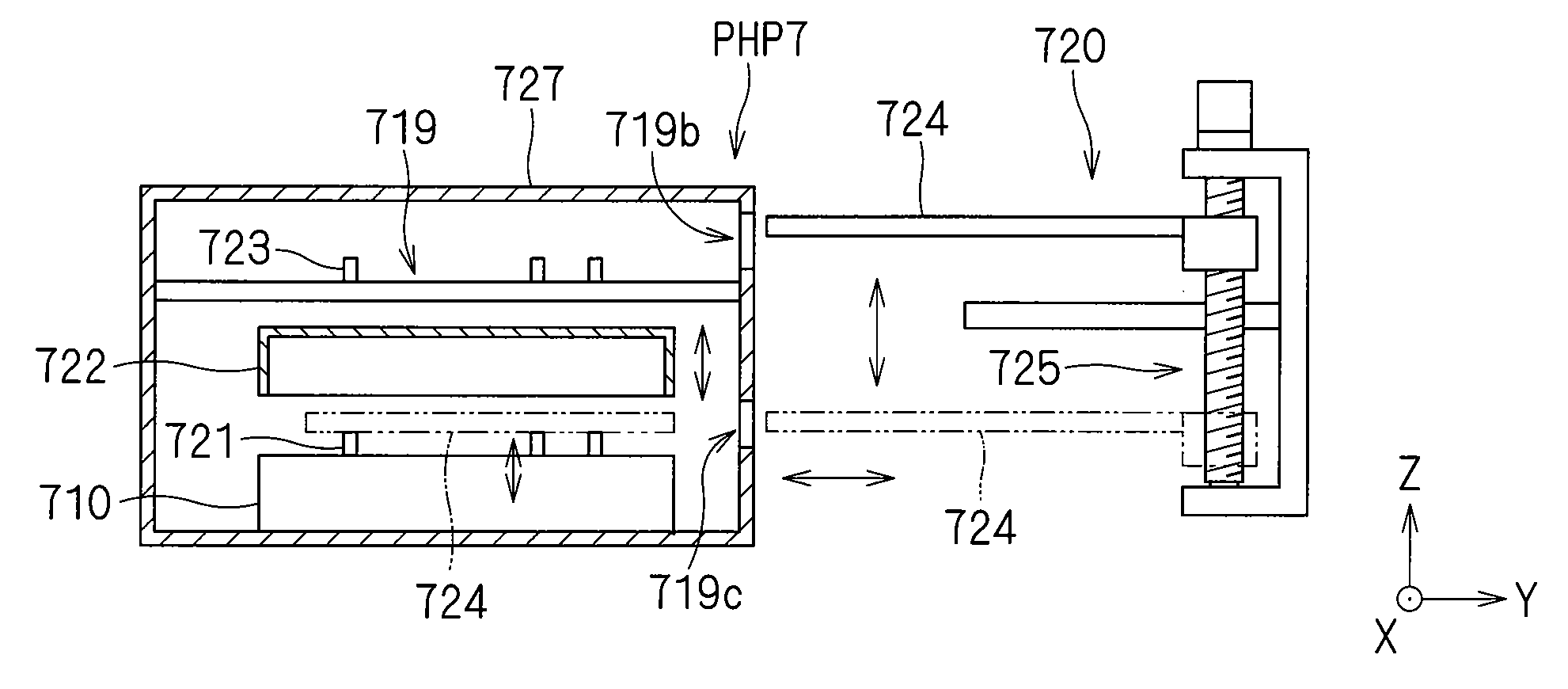
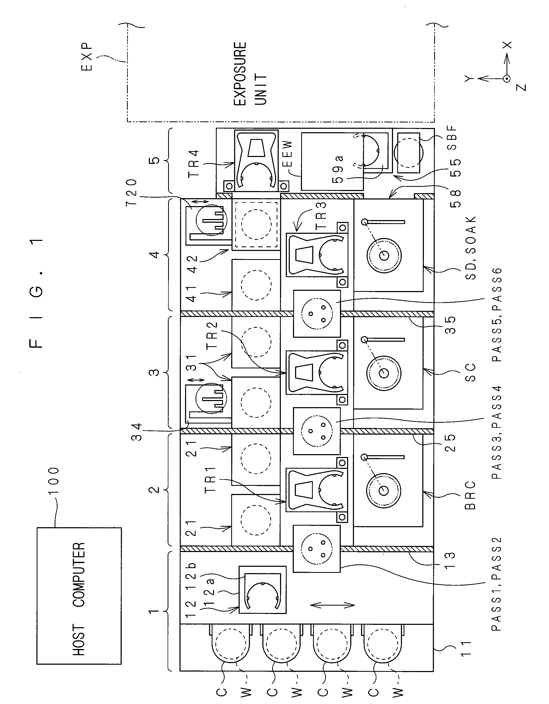
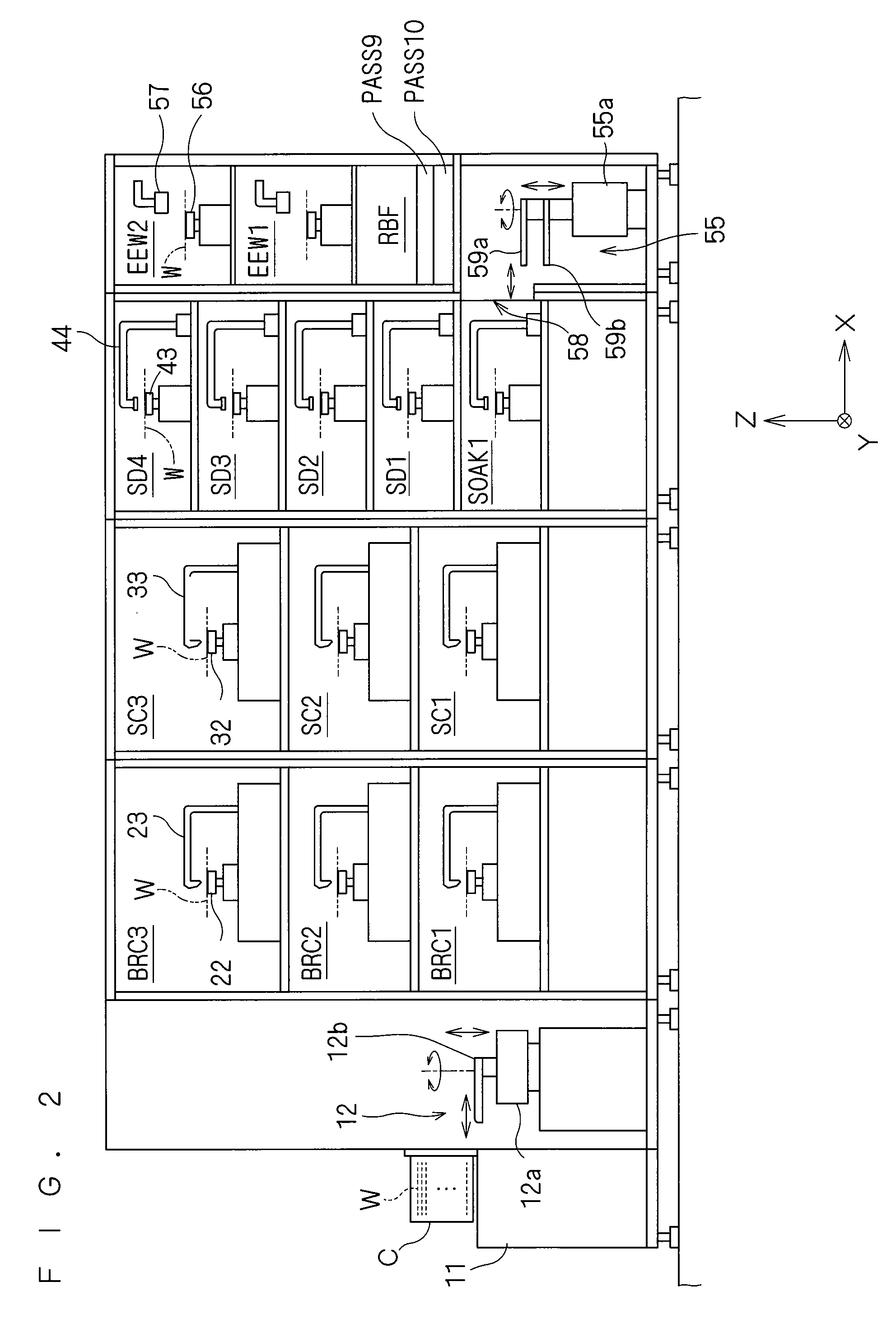
[0030]FIG. 1 is a plan view of a substrate processing apparatus according to the present invention. FIG. 2 is a front view of a liquid processing part in the substrate processing apparatus. FIG. 3 is a front view of a thermal processing part in the substrate processing apparatus. FIG. 4 is a view showing a construction around substrate rest parts. An XYZ rectangular coordinate system in which an XY plane is defined as the horizontal plane and a Z axis is defined to extend in the vertical direction is additionally shown in FIG. 1 and the subsequent figures for purposes of clarifying the directional relationship therebetween.
[0031] The substrate processing apparatus according to the preferred embodiment is an apparatus (a so-called coater-and-developer) for forming an anti-reflective film and a photoresist film on substrates such as semiconductor wafers by ...
PUM
| Property | Measurement | Unit |
|---|---|---|
| time | aaaaa | aaaaa |
| interprocess time interval | aaaaa | aaaaa |
| presence time | aaaaa | aaaaa |
Abstract
Description
Claims
Application Information