Plasma ashing method

a technology of ashing and plasma, applied in the field of plasma ashing, can solve the problems of limitation in further suppressing damage, etc., and achieve the effect of suppressing damage to low-k film or underlying film formation

Inactive Publication Date: 2007-03-15
TOKYO ELECTRON LTD
View PDF8 Cites 15 Cited by
  • Summary
  • Abstract
  • Description
  • Claims
  • Application Information

AI Technical Summary

Benefits of technology

[0012] It is, therefore, an object of the present invention to provide a plasma ashing method capable of suppressing a d

Problems solved by technology

However, when a fluorine-containing gas (for example, a CF based processing gas) is used as the processing gas in the etching process, there is a concern that reaction products such as fluorine polymer (for example, CF based polymer) will be deposited on inner walls of the processing chamber.
However, in a case where a layer including a low-k film (hereinafter referred to as a “low-k film”) is formed under a resist film, there is the concern that the low-k film

Method used


Image

  • Plasma ashing method
  • Plasma ashing method
  • Plasma ashing method

Examples


first embodiment

[0041] (Example of a Configuration of a Plasma Processing Apparatus in Accordance with Present Invention)

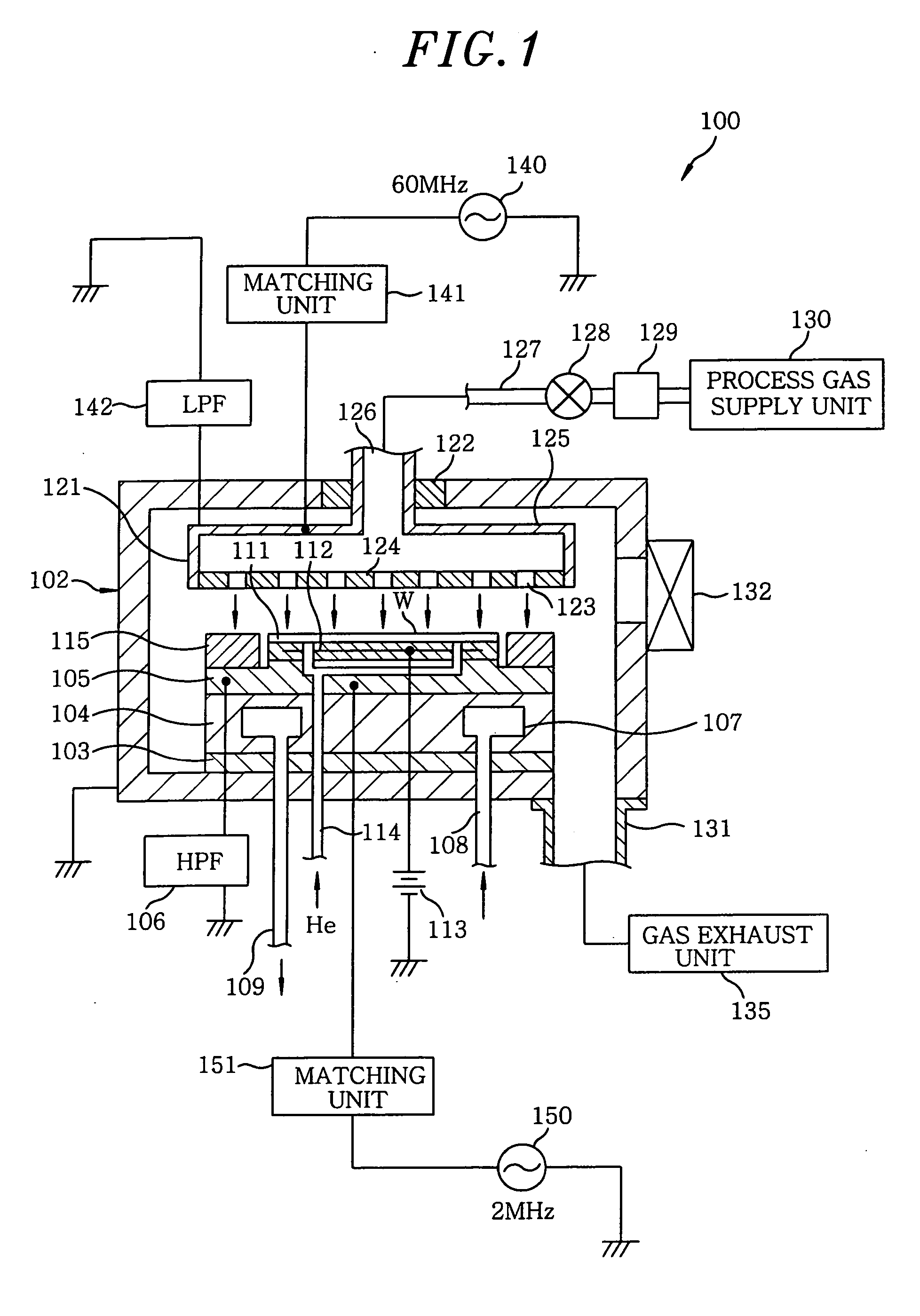
[0042] First, an example of the configuration of a plasma processing apparatus 100 in accordance with a first embodiment of the present invention will be described with reference to the drawing. FIG. 1 illustrates the schematic configuration of the plasma processing apparatus 100 in accordance with the first embodiment. The plasma processing apparatus 100 includes an upper electrode as a first electrode, and a lower electrode as a second electrode, which is located to face the first electrode. This plasma processing apparatus is a parallel plate plasma processing apparatus.

[0043] As shown in FIG. 1, the plasma processing apparatus 100 has a processing chamber 102 that is formed of a processing container formed in a cylindrical shape the surface of which is made of anodized aluminum (alumite-treated aluminum), wherein the processing chamber 102 is grounded. A susceptor support 10...

second embodiment

[0140] (Example of Configuration of Plasma Processing Apparatus in Accordance with Second Embodiment)

[0141] Next, an example of the configuration of the plasma processing apparatus in accordance with a second embodiment of the present invention is described with reference to the drawing. FIG. 15 shows the schematic configuration of a plasma processing apparatus 300 in accordance with a second embodiment. The plasma processing apparatus 300 shown in FIG. 15 applies the first high frequency power (plasma generation high frequency power) having a comparatively high frequency of, for example, 400 MHz and the second high frequency power (high frequency power for bias voltage generation) having a comparatively low frequency of, for example, 3.2 MHz to an electrode (lower electrode) which is also used as a loader, in an overlapping fashion. The plasma ashing method in accordance with the present invention can be also applied to such a type of plasma processing apparatus 300.

[0142] The pla...


PUM

PropertyMeasurementUnit
Pressureaaaaaaaaaa
Pressureaaaaaaaaaa
Poweraaaaaaaaaa

Abstract

A plasma ashing method is used for removing a patterned resist film in a processing chamber after etching a portion of a low-k film from an object to be processed in the processing chamber by using the patterned resist film as a mask. The method includes a first step of supplying a reaction product removal gas including at least CO2 gas into the processing chamber, generating plasma of the reaction product removal gas by applying a high frequency power for the plasma generation, and removing reaction products deposited on an inner wall of the processing chamber; and a second step of supplying an ashing gas into the processing chamber, generating plasma of the ashing gas by applying a high frequency power for the plasma generation, and removing the resist film.

Description

CROSS-REFERENCE TO RELATED APPLICATIONS [0001] This document claims priority to Japanese Patent Application No. 2005-262713, filed on Sep. 9, 2005 and U.S. Provisional Application No. 60 / 722,966, filed on Oct. 4, 2005, the entire content of which are hereby incorporated by reference. [0002] 1. Field of the Invention [0003] The present invention relates to a plasma ashing method of removing a resist film from an object to be processed. [0004] 1. Background of the Invention [0005] In an exemplary semiconductor manufacturing process, an etching process is performed by using a predetermined processing gas while using as a mask a resist film having trenches and holes, which is patterned on the surface of an object to be processed such as a semiconductor wafer (hereinafter referred to as a “wafer”), and then an ashing process is performed to remove the remaining resist film. [0006] For such an ashing process, a method of ashing and removing a resist film (plasma ashing method) by using a ...

Claims


Application Information

Patent Timeline
IPC IPC(8): H01L21/302
CPCG03F7/427H01L21/67069H01L21/02063
Inventor TAHARA, SHIGERUHOSHI, NAOTSUGU
Owner TOKYO ELECTRON LTD
Why Eureka
Try Eureka