Ultrafast laser direct writing method for modifying existing microstructures on a submicron scale

a microstructure and ultrafast laser technology, applied in the field of ultrafast laser direct writing method for modifying existing microstructures on a submicron scale, can solve the problems of complex lithographic methods, high-cost techniques usually require stringent environmental conditions, and complicated manufacturing of materials

Inactive Publication Date: 2007-03-22
LI MING +1
View PDF10 Cites 14 Cited by
  • Summary
  • Abstract
  • Description
  • Claims
  • Application Information

AI Technical Summary

Benefits of technology

[0019] Yet another exemplary embodiment of the present invention is a method for forming a defect in a photonic crystal. A photonic crystal work piece is provided. The top surface of the photonic crystal work piece includes an alignment section and a photonic crystal section. The photonic crystal section has a number of air holes formed in an interstitial material. Each of the air holes has a diameter less than an illumination wavelength used to image the device during defect formation and the centers of two of the air holes are a predetermined distance apart. An origin mark is ablated in the alignment section of the photonic crystal work piece with a micro-machining laser. The top surface of the photonic crystal work piece is illuminated with light having the illumination wavelength and imaged with a digital camera. This produces an alignment image of the top surface which includes a matrix of pixels. The alignment image is scaled such that each pixel has a width corresponding to a constant distance on the top surface of the photonic crystal work piece, which is less than half of the illumination wavelength. The constant distance is determined based on a number of pixels in the alignment image between the centers of the two air holes that are separated by the predetermined distance. The location of the center of the calibration mark in the alignment image is determined and an image coordinate system for the top surface of the photonic crystal work piece is defined using the location of the origin mark in the alignment image, the matrix of pixels, and the constant distance. Coordinates of the centers of the air holes of the photonic crystal work piece in the image coordinate system are determined using the alignment image. Also, initial coordinates of the beam spot of the micro-machining laser in the image coordinate system are determined using the location of the origin mark in the alignment image. The beam spot of the micro-machining laser is then aligned over a defect location of the photonic crystal section using the coordinates of the air holes and the initial coordinates of the beam spot. Interstitial material at the defect location of the photonic crystal section is machined with the micro-machining laser to form the defect. A still further exemplary embodiment of the present invention is a method for improving

Problems solved by technology

The feature sizes used to form photonic crystals and the precise alignment requirements of these features complicate manufacture of these materials.
One challenge in producing micro-circuitry is preventing shorts between components and nano-wires which are located ever closer together.
These high-cost techniques usually require stringent environmental conditions, such as high vacuum or clean room condition.
All the lithographic methods require a series of complicated procedures, which involve generating multiple masks and using photoresist.
Still alignment of a laser beam to nanostructures on existing microstructures is a difficult issue.

Method used


Image

  • Ultrafast laser direct writing method for modifying existing microstructures on a submicron scale
  • Ultrafast laser direct writing method for modifying existing microstructures on a submicron scale
  • Ultrafast laser direct writing method for modifying existing microstructures on a submicron scale

Examples


Embodiment Construction

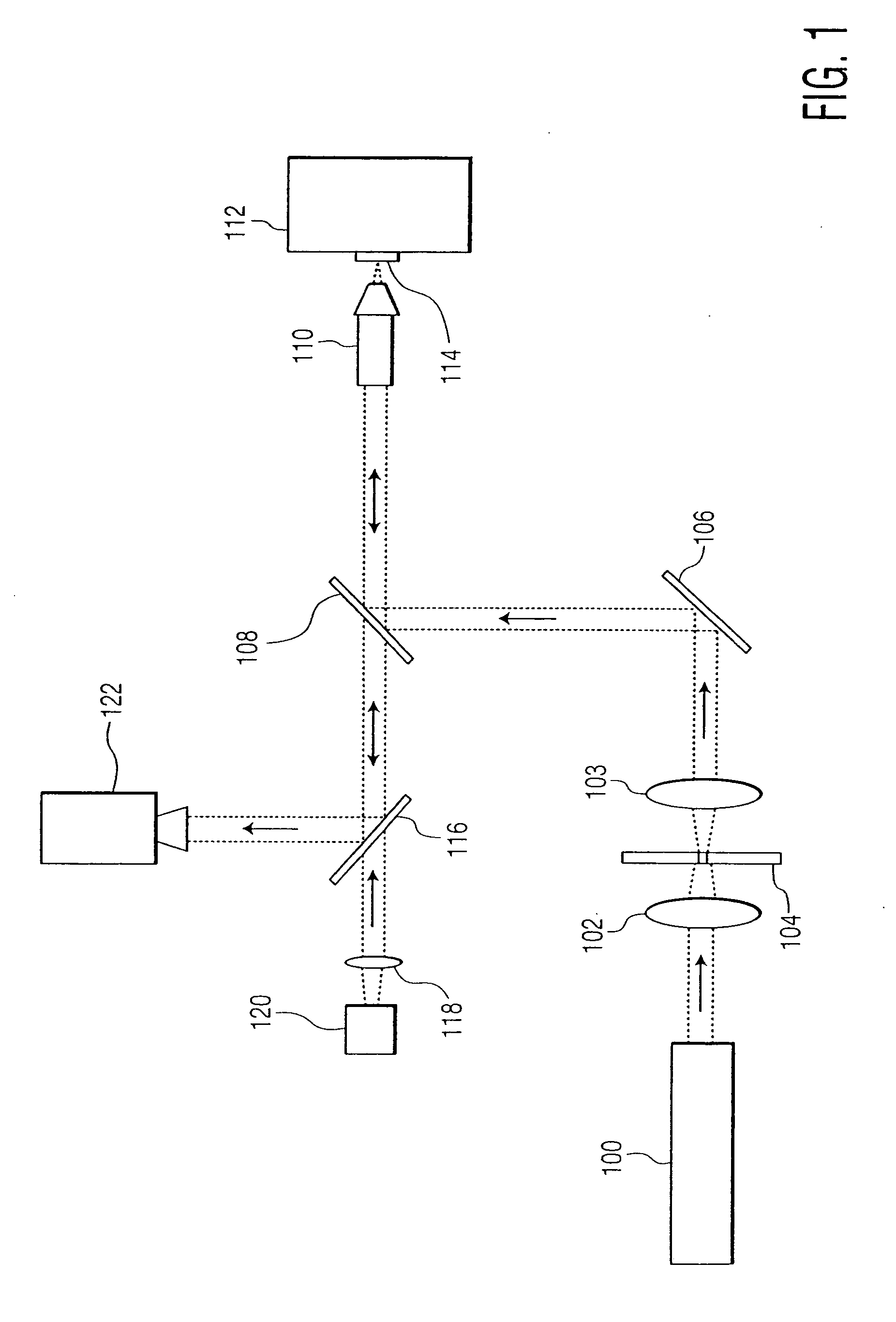
[0036]FIG. 1 illustrates a simplified block diagram of an exemplary laser micro-machining system that may be used in any of the exemplary methods of the present invention. This exemplary system includes laser source 100, work piece holder 112, work piece illumination source 120 and digital camera 122 to image the work piece, as well as numerous optical elements to direct and shape the optical beams. The optical beams are shown as dotted lines with arrows indicating the direction(s) of light propagating in the different sections of the exemplary system.

[0037] In this exemplary system, laser source 100 may desirably include an ultrafast laser, an excimer laser, or another type of laser typically used for laser machining applications. Harmonic generating crystals and / or amplifiers may be used within this component. Desirably, a frequency-doubled, 150 fs Ti:Sapphire laser (for example a Clark MXR CPA2000) may be used as the laser. Laser source 100 may also desirably include optics to c...


PUM

PropertyMeasurementUnit
pitch sizeaaaaaaaaaa
sizesaaaaaaaaaa

Abstract

A method for pre-calibration of a laser micro-machining system to achieve alignment tolerances greater than the diffraction limit of an illumination wavelength. A blank is mounted in the system, such that the beam spot is incident on its top surface. Two marks are ablated in the blank. The centers of the marks are a predetermined distance apart. The blank is illuminated with light and imaged with a digital camera. The resulting image is scaled such that each pixel has a width corresponding to a distance on the imaged surface, which is less than half of the illumination wavelength. The number of pixels between the centers of the marks determines this distance. The locations of the marks in the image are determined and a coordinate system is defined for surfaces imaged by the digital camera. Coordinates of the beam spot in this coordinate system are also determined using the second mark.

Description

[0001] This application claims the benefit of U.S. patent application Ser. No. 10 / 790,401, filed Mar. 1, 2004 the contents of which are incorporated herein by reference.FIELD OF THE INVENTION [0002] The present invention concerns a simplified method for micro- and nano-machining of submicron features on existing microstructures. This method may also allow mass customization of generic electronic and mechanical microstructures. BACKGROUND OF THE INVENTION [0003] As products get smaller and smaller, there is stronger and stronger demand for micro-electrical-mechanical systems (MEMS), micro-optical devices and photonic crystals. With this demand, there is an associated increased interest in micro- and nano-machining. There are numerous possible applications for MEMS. As a breakthrough technology, allowing unparalleled synergy between previously unrelated fields such as biology and microelectronics, many new MEMS applications have emerged and many more may emerge in the near future, exp...

Claims


Application Information

Patent Timeline
Patent Type & Authority Applications(United States)
IPC IPC(8): B23K26/38B81C99/00B23K26/04B23K26/06B23K26/067B81B1/00
CPCB23K26/041B23K26/0613B23K26/0635B23K26/4095B23K26/381B23K26/383B23K26/067B23K26/40B23K26/042B23K26/0624B23K26/382B23K26/384B23K2101/35
Inventor LI, MINGISHIZUKA, MAKOTO
Owner LI MING
Why Eureka
Try Eureka