
Electrode for mass spectrometry

Active Publication Date: 2007-03-22
AGILENT TECH AUSTRALIA M
View PDF3 Cites 8 Cited by
  • Summary
  • Abstract
  • Description
  • Claims
  • Application Information

AI Technical Summary

Benefits of technology

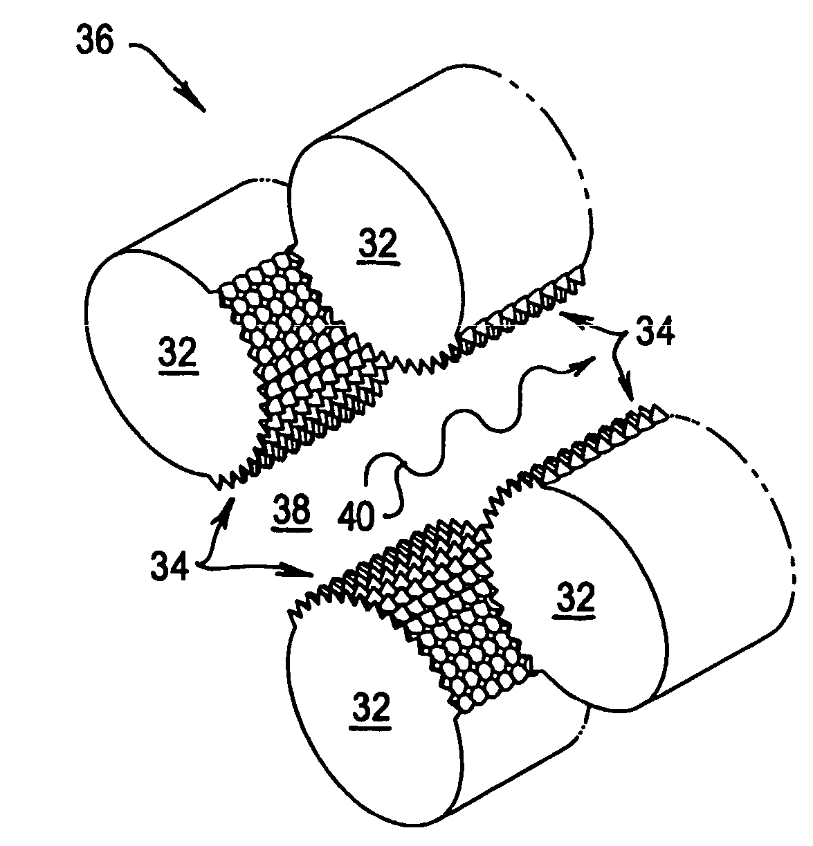
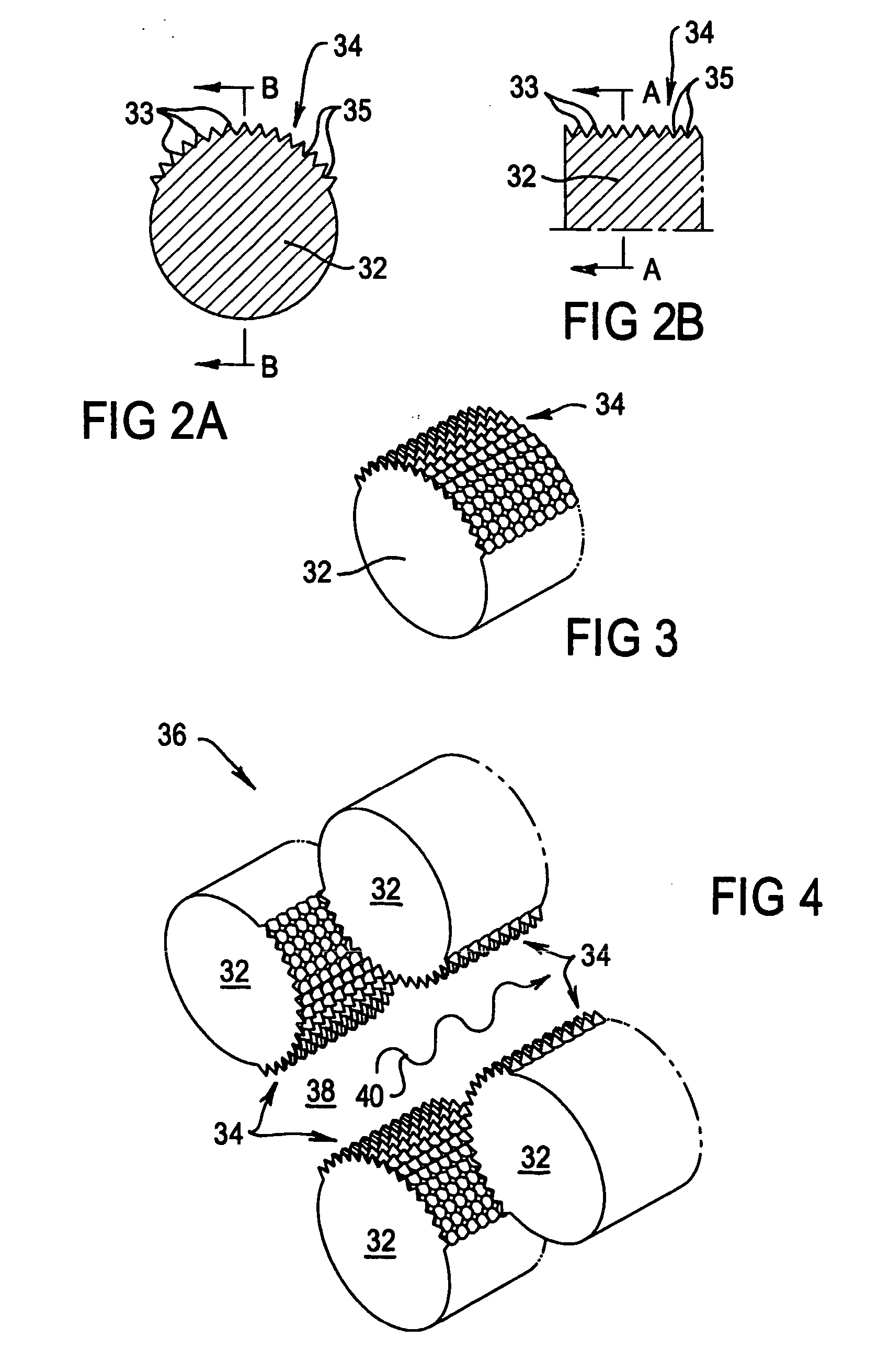
[0007] wherein the surface portion is relatively rough to provide projections and cavities for reducing deposition of dielectric substances onto the surface portion.
[0008] It has been found that deposition of a dielectric film is less likely to occur when the surface portion of the electrode that defines an equipotential boundary for an electric field is not polished as for prior art electrodes, but instead is made rough by inclusion or projections and cavities.
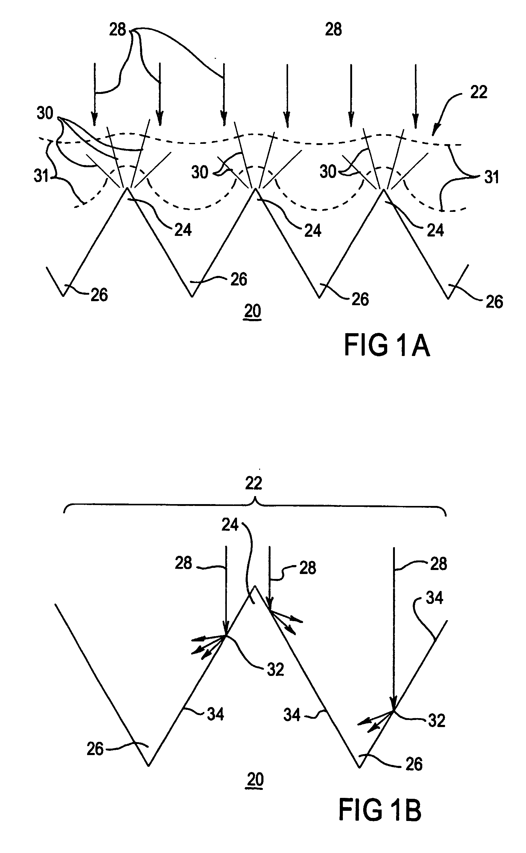
[0009] Preferably the projections have a shape or shapes such that they reduce in size outwardly of the surface portion whereby they have at least one sloped side surface for providing an increased probability that the charged particles will strike such side surfaces at an angle thereto. It is considered that this feature assists to reduce deposition of dielectric substances on the projections, as will be explained below.
[0011] According to the invention, the “degree of roughness” of the surface may be quite pronounced, for example a distance of approximately 0.5 mm from the peak of a projection to the base of a cavity has provided significantly improved results compared to a prior art polished surface electrode.
[0012] Preferably the surface portion in question of an electrode according to the invention is provided with a helical formation such as a screw thread to provide the roughness.

Problems solved by technology

However such electrodes are subject to deposition of non-conducting (dielectric) substances thereon.
This surface charge causes unstable performance of the mass spectrometer.
These dielectric films can be highly detrimental to the stability of the instrument's performance.

Method used


Image

  • Electrode for mass spectrometry
  • Electrode for mass spectrometry
  • Electrode for mass spectrometry

Examples


Embodiment Construction

[0022] It is known that dielectric film when deposited on electrodes in a vacuum system of a mass spectrometer can cause build-up of electrical charges on the affected surfaces. This causes changes in the electrical fields around the electrode causing changes in the performance characteristics of the mass spectrometer. The present invention is based on the observation that film deposition is less likely to happen when the surface is not polished, but is rough. It is believed that when an electrode surface exposed to a flux of potentially contaminating particles consists of a combination of cavities and projections (which may be micro-cavities and micro-pinnacles), then that surface is in a favourable condition for dispersing initial deposits of contaminating film around the projections in such a way that at least the projections tend to stay relatively clean. As long as the projections are relatively clean, the electric field around the electrode remains stable and causes no change ...


PUM


Abstract

An electrode for use in a reduced pressure region in a mass spectrometer whereby the electrode is subject to deposition of dielectric (non-conducting) substances thereon, which can cause unstable performance of the mass spectrometer. The surface portion of the electrode that is for providing an equipotential boundary of an electric field for influencing charged particles is made rough, in contrast to the prior art of providing a polished surface. The rough surface provides projections and cavities, which may have a regular or irregular occurrence, which it has been found significantly reduces the deposition of dielectric substances from the charged particles thereon. A preferred structure is for a rod electrode (42) to have a screw thread (44) formed thereon whereby the thread crests (43) along the rod electrode provide projections (43) and the thread roots (45) provide cavities.

Description

TECHNICAL FIELD [0001] The present invention relates to an electrode for use in a region of a mass spectrometer where the electrode is subject to deposition of dielectric substances thereon. Generally the region of the mass spectrometer will be a reduced pressure region. The electrode may be part of a mass analyser, ion optics system or ion guide, ion detector or source to spectrometer interface in a mass spectrometer, the mass spectrometer being used in conjunction with, for example, an inductively coupled plasma, microwave induced plasma, liquid chromatograph, gas chromatograph or laser ablation. BACKGROUND [0002] The following discussion of the background to the invention is included to explain the context of the invention. This is not to be taken as an admission that any of the material referred to was published, known or part of the common general knowledge in the art as at the priority date established by the present application. [0003] Electrodes within a reduced pressure reg...

Claims


Application Information

Patent Timeline
IPC IPC(8): H01J49/00H01J49/02H01J49/06H01J49/26H01J49/42
CPCH01J49/4215H01J49/063
Inventor KALINITCHENKO, IOURI
Owner AGILENT TECH AUSTRALIA M
Learn More